- 您现在的位置:买卖IC网 > PDF目录8351 > 74LCX112M (Fairchild Semiconductor)IC FLIP FLOP DUAL JK NEG 16SOIC PDF资料下载
参数资料
| 型号: | 74LCX112M |
| 厂商: | Fairchild Semiconductor |
| 文件页数: | 1/9页 |
| 文件大小: | 0K |
| 描述: | IC FLIP FLOP DUAL JK NEG 16SOIC |
| 标准包装: | 48 |
| 系列: | 74LCX |
| 功能: | 设置(预设)和复位 |
| 类型: | JK 型 |
| 输出类型: | 差分 |
| 元件数: | 2 |
| 每个元件的位元数: | 1 |
| 频率 - 时钟: | 150MHz |
| 延迟时间 - 传输: | 7ns |
| 触发器类型: | 负边沿 |
| 输出电流高,低: | 24mA,24mA |
| 电源电压: | 2 V ~ 3.6 V |
| 工作温度: | -40°C ~ 85°C |
| 安装类型: | 表面贴装 |
| 封装/外壳: | 16-SOIC(0.154",3.90mm 宽) |
| 包装: | 管件 |
2001 Fairchild Semiconductor Corporation
DS012424
www.fairchildsemi.com
June 1998
Revised February 2001
7
4
LCX1
12
Low
V
o
lt
age
Dual
J-K
Negati
ve
E
d
ge-T
ri
gger
e
d
Fli
p
-Fl
op
w
ith
5V
T
o
le
ra
nt
Input
s
74LCX112
Low Voltage Dual J-K Negative Edge-Triggered Flip-Flop
with 5V Tolerant Inputs
General Description
The LCX112 is a dual J-K flip-flop. Each flip-flop has inde-
pendent J, K, PRESET, CLEAR, and CLOCK inputs with Q,
Q outputs. These devices are edge sensitive and change
state on the negative going transition of the clock pulse.
Clear and preset are independent of the clock and accom-
plished by a low logic level on the corresponding input.
LCX devices are designed for low voltage (3.3V or 2.5)
operation with the added capability of interfacing to a 5V
signal environment.
The 74LCX112 is fabricated with advanced CMOS technol-
ogy to achieve high speed operation while maintaining
CMOS low power dissipation.
Features
s 5V tolerant inputs
s 2.3V–3.6V VCC specifications provided
s 7.5 ns tPD max (VCC = 3.3V), 10 A ICC max
s Power down high impedance inputs and outputs
s
±24 mA output drive (V
CC = 3.0V)
s Implements patented noise/EMI reduction circuitry
s Latch-up performance exceeds 500 mA
s ESD performance:
Human body model
> 2000V
Machine model
> 2000V
Ordering Code:
Devices also available in Tape and Reel. Specify by appending suffix letter “X” to the ordering code.
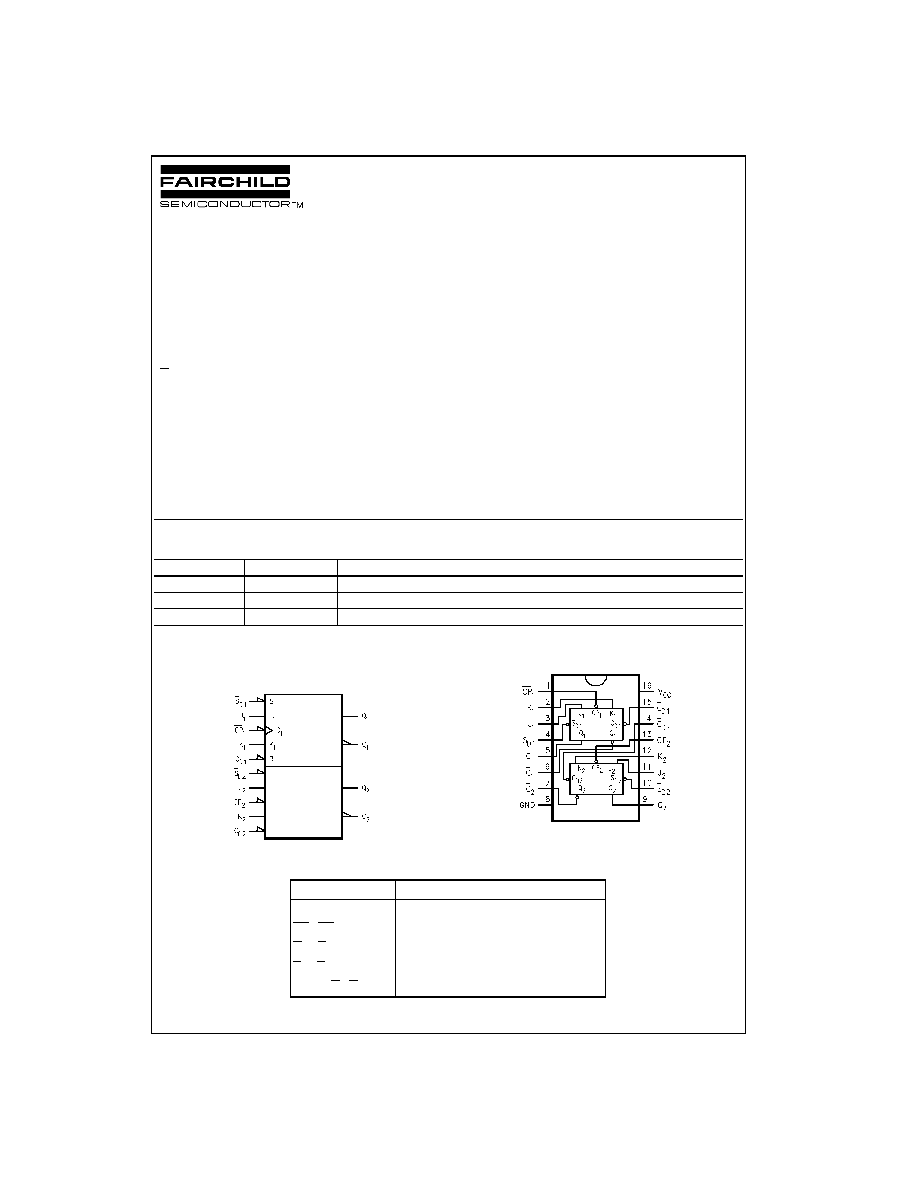
Logic Symbol
IEEE/IEC
Connection Diagram
Pin Descriptions
Order Number
Package Number
Package Description
74LCX112M
M16A
16-Lead Small Outline Integrated Circuit (SOIC), JEDEC MS-012, 0.150 Narrow
74LCX112SJ
M16D
16-Lead Small Outline Package (SOP), EIAJ TYPE II, 5.3mm Wide
74LCX112MTC
MTC16
16-Lead Thin Shrink Small Outline Package (TSSOP), JEDEC MO-153, 4.4mm Wide
Pin Names
Description
J1, J2, K1, K2
Data Inputs
CP1, CP2
Clock Pulse Inputs (Active Falling Edge)
CD1, CD2
Direct Clear Inputs (Active LOW)
SD1, SD2
Direct Set Inputs (Active LOW)
Q1, Q2, Q1, Q2
Outputs
相关PDF资料 |
PDF描述 |
|---|---|
| VI-26J-MV-F2 | CONVERTER MOD DC/DC 36V 150W |
| VI-26J-MV-F1 | CONVERTER MOD DC/DC 36V 150W |
| MC74HC377ADTR2G | IC FLIP/FLOP OCTL D-TYPE 20TSSOP |
| VI-26B-MV-F3 | CONVERTER MOD DC/DC 95V 150W |
| VI-26B-MV-F2 | CONVERTER MOD DC/DC 95V 150W |
相关代理商/技术参数 |
参数描述 |
|---|---|
| 74LCX112M_Q | 功能描述:触发器 J-K Neg Flip-Flop RoHS:否 制造商:Texas Instruments 电路数量:2 逻辑系列:SN74 逻辑类型:D-Type Flip-Flop 极性:Inverting, Non-Inverting 输入类型:CMOS 输出类型: 传播延迟时间:4.4 ns 高电平输出电流:- 16 mA 低电平输出电流:16 mA 电源电压-最大:5.5 V 最大工作温度:+ 85 C 安装风格:SMD/SMT 封装 / 箱体:X2SON-8 封装:Reel |
| 74LCX112MTC | 功能描述:触发器 J-K Neg Flip-Flop RoHS:否 制造商:Texas Instruments 电路数量:2 逻辑系列:SN74 逻辑类型:D-Type Flip-Flop 极性:Inverting, Non-Inverting 输入类型:CMOS 输出类型: 传播延迟时间:4.4 ns 高电平输出电流:- 16 mA 低电平输出电流:16 mA 电源电压-最大:5.5 V 最大工作温度:+ 85 C 安装风格:SMD/SMT 封装 / 箱体:X2SON-8 封装:Reel |
| 74LCX112MTC_Q | 功能描述:触发器 J-K Neg Flip-Flop RoHS:否 制造商:Texas Instruments 电路数量:2 逻辑系列:SN74 逻辑类型:D-Type Flip-Flop 极性:Inverting, Non-Inverting 输入类型:CMOS 输出类型: 传播延迟时间:4.4 ns 高电平输出电流:- 16 mA 低电平输出电流:16 mA 电源电压-最大:5.5 V 最大工作温度:+ 85 C 安装风格:SMD/SMT 封装 / 箱体:X2SON-8 封装:Reel |
| 74LCX112MTCX | 功能描述:触发器 J-K Neg Flip-Flop RoHS:否 制造商:Texas Instruments 电路数量:2 逻辑系列:SN74 逻辑类型:D-Type Flip-Flop 极性:Inverting, Non-Inverting 输入类型:CMOS 输出类型: 传播延迟时间:4.4 ns 高电平输出电流:- 16 mA 低电平输出电流:16 mA 电源电压-最大:5.5 V 最大工作温度:+ 85 C 安装风格:SMD/SMT 封装 / 箱体:X2SON-8 封装:Reel |
| 74LCX112MX | 功能描述:触发器 J-K Neg Flip-Flop RoHS:否 制造商:Texas Instruments 电路数量:2 逻辑系列:SN74 逻辑类型:D-Type Flip-Flop 极性:Inverting, Non-Inverting 输入类型:CMOS 输出类型: 传播延迟时间:4.4 ns 高电平输出电流:- 16 mA 低电平输出电流:16 mA 电源电压-最大:5.5 V 最大工作温度:+ 85 C 安装风格:SMD/SMT 封装 / 箱体:X2SON-8 封装:Reel |
发布紧急采购,3分钟左右您将得到回复。