- 您现在的位置:买卖IC网 > PDF目录8317 > 74LCX14MTC (Fairchild Semiconductor)IC INVERTER HEX SCHMT IN 14TSSOP PDF资料下载
参数资料
| 型号: | 74LCX14MTC |
| 厂商: | Fairchild Semiconductor |
| 文件页数: | 7/13页 |
| 文件大小: | 0K |
| 描述: | IC INVERTER HEX SCHMT IN 14TSSOP |
| 标准包装: | 94 |
| 系列: | 74LCX |
| 逻辑类型: | 逆变器,缓冲器 |
| 电路数: | 6 |
| 输入数: | 1 |
| 特点: | 施密特触发器 |
| 电源电压: | 2 V ~ 3.6 V |
| 电流 - 静态(最大值): | 10µA |
| 输出电流高,低: | 24mA,24mA |
| 逻辑电平 - 低: | 0.4 V ~ 0.6 V |
| 逻辑电平 - 高: | 1.7 V ~ 2.2 V |
| 额定电压和最大 CL 时的最大传播延迟: | 6.5ns @ 3.3V,50pF |
| 工作温度: | -40°C ~ 85°C |
| 安装类型: | 表面贴装 |
| 供应商设备封装: | 14-TSSOP |
| 封装/外壳: | 14-TSSOP(0.173",4.40mm 宽) |
| 包装: | 管件 |
| 产品目录页面: | 1210 (CN2011-ZH PDF) |
1995 Fairchild Semiconductor Corporation
www.fairchildsemi.com
74LCX14
—
Lo
w
V
olta
g
e
He
x
In
ver
ter
with
5V
T
olerant
Sc
hmitt
T
rig
g
er
Inputs
Absolute Maximum Ratings
Stresses exceeding the absolute maximum ratings may damage the device. The device may not function or be
operable above the recommended operating conditions and stressing the parts to these levels is not recommended.
In addition, extended exposure to stresses above the recommended operating conditions may affect device reliability.
The absolute maximum ratings are stress ratings only.
Note:
2. IO Absolute Maximum Rating must be observed.
Recommended Operating Conditions(3)
The Recommended Operating Conditions table defines the conditions for actual device operation. Recommended
operating conditions are specified to ensure optimal performance to the datasheet specifications. Fairchild does not
recommend exceeding them or designing to absolute maximum ratings.
Note:
3. Unused inputs must be held HIGH or LOW. They may not float.
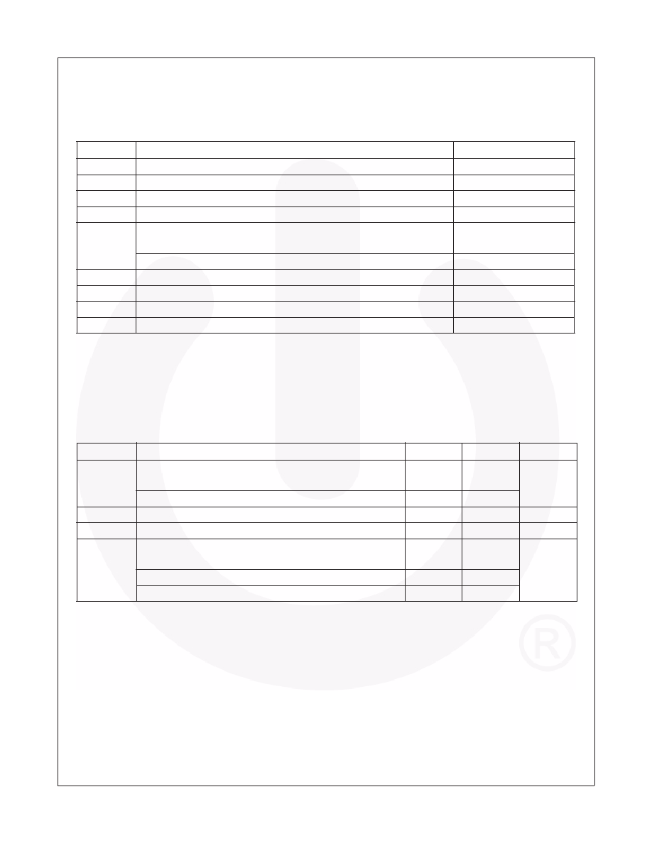
Symbol
Parameter
Rating
VCC
Supply Voltage
–0.5V to +7.0V
VI
DC Input Voltage
–0.5V to +7.0V
VO
DC Output Voltage, Output in HIGH or LOW State(2)
–0.5V to VCC + 0.5V
IIK
DC Input Diode Current, VI < GND
–50mA
IOK
DC Output Diode Current
VO < GND
–50mA
VO > VCC
+50mA
IO
DC Output Source/Sink Current
±50mA
ICC
DC Supply Current per Supply Pin
±100mA
IGND
DC Ground Current per Ground Pin
±100mA
TSTG
Storage Temperature
–65°C to +150°C
Symbol
Parameter
Min.
Max.
Units
VCC
Supply Voltage
Operating
2.0
3.6
V
Data Retention
1.5
3.6
VI
Input Voltage
0
5.5
V
VO
Output Voltage, HIGH or LOW State
0
VCC
V
IOH / IOL
Output Current
VCC = 3.0V–3.6V
±24
mA
VCC = 2.7V–3.0V
±12
VCC = 2.3V–2.7V
±8
74LCX14 Rev. 1.7.1
3
相关PDF资料 |
PDF描述 |
|---|---|
| MS3450W16-9A | CONN HSG RCPT 4POS WALLMNT PINS |
| MS27484E16F6SLC | CONN HSG PLUG 6POS STRGHT SCKT |
| MS27468T25F35AA | CONN HSG RCPT 128POS JAM NUT PIN |
| MS3450W22-14SLC | CONN HSG RCPT 19POS WALLMNT SCKT |
| MS3450W22-14BZ | CONN HSG RCPT 19POS WALLMNT SCKT |
相关代理商/技术参数 |
参数描述 |
|---|---|
| 74LCX14MTC_Q | 功能描述:变换器 Hex Inverter RoHS:否 制造商:NXP Semiconductors 电路数量:6 逻辑系列:74ABT 逻辑类型:BiCMOS 高电平输出电流:- 15 mA 低电平输出电流:20 mA 传播延迟时间:2.2 ns 电源电压-最大:5.5 V 电源电压-最小:4.5 V 最大工作温度:+ 85 C 最小工作温度:- 40 C 工作温度范围: 封装 / 箱体:DIP-14 封装:Tube |
| 74LCX14MTCX | 功能描述:变换器 Hex Inverter RoHS:否 制造商:NXP Semiconductors 电路数量:6 逻辑系列:74ABT 逻辑类型:BiCMOS 高电平输出电流:- 15 mA 低电平输出电流:20 mA 传播延迟时间:2.2 ns 电源电压-最大:5.5 V 电源电压-最小:4.5 V 最大工作温度:+ 85 C 最小工作温度:- 40 C 工作温度范围: 封装 / 箱体:DIP-14 封装:Tube |
| 74LCX14MTCX | 制造商:Fairchild Semiconductor Corporation 功能描述:Schmitt Inverter Logic IC |
| 74LCX14MTCX_NL | 功能描述:变换器 FINISHED GOOD RoHS:否 制造商:NXP Semiconductors 电路数量:6 逻辑系列:74ABT 逻辑类型:BiCMOS 高电平输出电流:- 15 mA 低电平输出电流:20 mA 传播延迟时间:2.2 ns 电源电压-最大:5.5 V 电源电压-最小:4.5 V 最大工作温度:+ 85 C 最小工作温度:- 40 C 工作温度范围: 封装 / 箱体:DIP-14 封装:Tube |
| 74LCX14MTR | 功能描述:变换器 Hex Schmitt Trig Inv RoHS:否 制造商:NXP Semiconductors 电路数量:6 逻辑系列:74ABT 逻辑类型:BiCMOS 高电平输出电流:- 15 mA 低电平输出电流:20 mA 传播延迟时间:2.2 ns 电源电压-最大:5.5 V 电源电压-最小:4.5 V 最大工作温度:+ 85 C 最小工作温度:- 40 C 工作温度范围: 封装 / 箱体:DIP-14 封装:Tube |
发布紧急采购,3分钟左右您将得到回复。