参数资料
| 型号: | 74LCX540MSA |
| 厂商: | Fairchild Semiconductor |
| 文件页数: | 4/14页 |
| 文件大小: | 0K |
| 描述: | IC INVERTER 8-INPUT 20SSOP |
| 标准包装: | 66 |
| 系列: | 74LCX |
| 逻辑类型: | 逆变器,缓冲器 |
| 电路数: | 1 |
| 输入数: | 8 |
| 特点: | 三态 |
| 电源电压: | 2 V ~ 3.6 V |
| 电流 - 静态(最大值): | 10µA |
| 输出电流高,低: | 24mA,24mA |
| 逻辑电平 - 低: | 0.7 V ~ 0.8 V |
| 逻辑电平 - 高: | 1.7 V ~ 2 V |
| 额定电压和最大 CL 时的最大传播延迟: | 6.5ns @ 3.3V,50pF |
| 工作温度: | -40°C ~ 85°C |
| 安装类型: | 表面贴装 |
| 供应商设备封装: | 20-SSOP |
| 封装/外壳: | 20-SSOP(0.209",5.30mm 宽) |
| 包装: | 管件 |
2010 Fairchild Semiconductor Corporation
www.fairchildsemi.com
FAB1200 Rev 1.2.7
12
FAB
12
00
—
Ground
-Re
ferenc
ed
Class
-G
He
adp
hone
Ampli
fi
er
wi
th
I
n
tegrated
Buck
Co
nvert
er
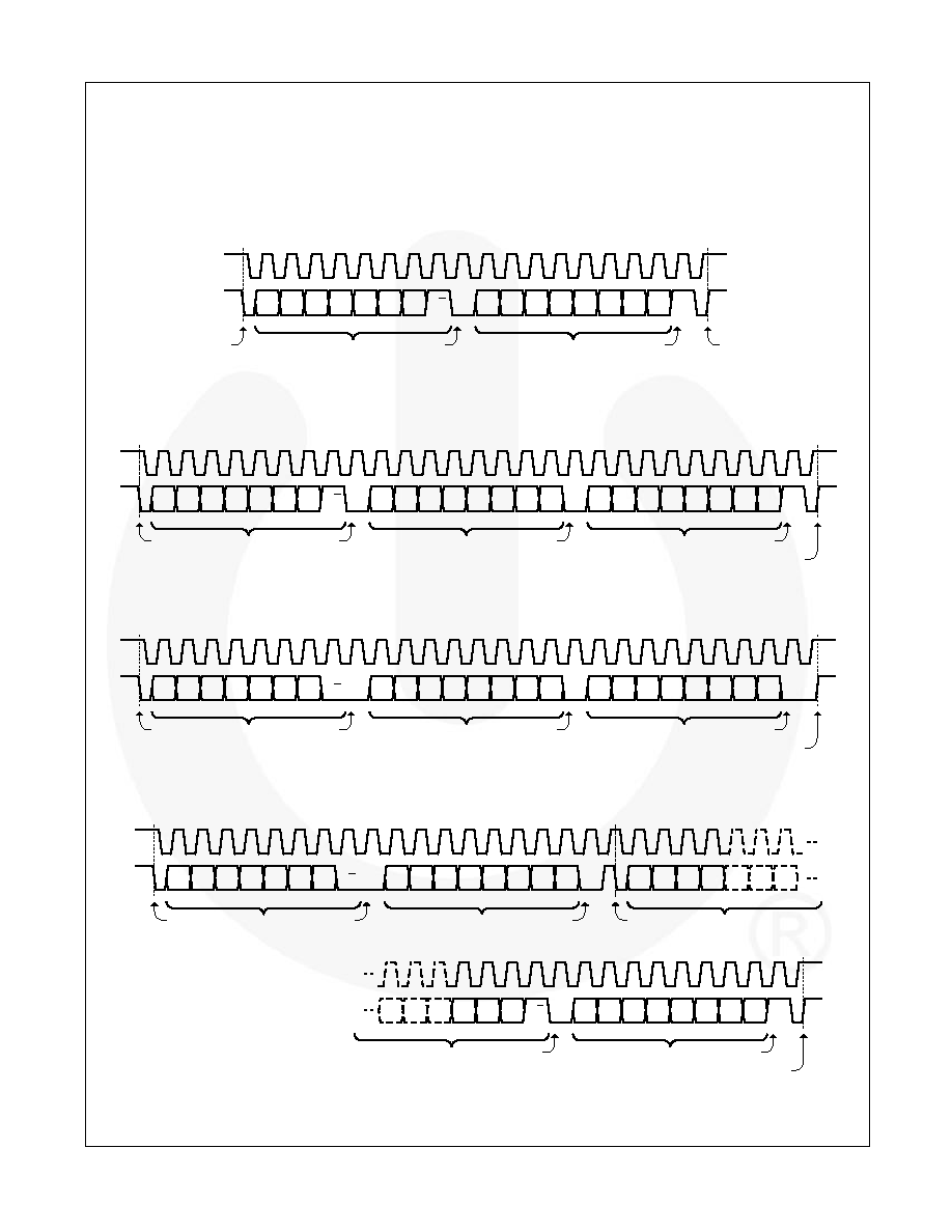
Writing
All writes must be preceded by a pointer set, even if the
pointer is already pointing to the desired register.
Immediately following the pointer set, the master must
begin
transmitting
the
data
to
be
written.
After
transmitting each byte of data, the master must release
the SDA line for one clock cycle to allow the FAB1200 to
acknowledge receiving the byte. The write operation
should be terminated by a STOP condition from the
master (see Figure 21).
As with reading, the master can write multiple bytes by
continuing to send data. The FAB1200 increments the
pointer by ones and accept data for the next register.
The master indicates the last data byte by issuing a
STOP condition.
SDA
SCL
D3
D7
D6
D5
D4
D2
D1
D0
A3
A7
A6
A5
A4
A2
A1
ACK
NACK
R/W
Slave Address
(from Master)
Data
(from Slave)
ACK
(from Slave)
NACK
(from Master)
START
(from Master)
STOP
(from Master)
Figure 19. I
2C Read
SDA
SCL
D3
D7
D6
D5
D4
D2
D1
D0
A3
A7
A6
A5
A4
A2
A1
ACK
R/W
Slave Address
(from Master)
Data
(from Slave)
ACK
(from Slave)
ACK
(from Master)
D3
D7
D6
D5
D4
D2
D1
D0
ACK
NACK
Data
(from Slave)
NACK
(from Master)
STOP
(from Master)
START
(from Master)
Figure 20. I
2C Multiple-Byte Read
P3
P7
P6
P5
P4
P2
P1
P0
A3
A7
A6
A5
A4
A2
A1
R/W
ACK
SDA
SCL
ACK
(from Slave)
Slave Address
(from Master)
Pointer
(from Master)
D3
D7
D6
D5
D4
D2
D1
D0
ACK
Data
(from Master)
ACK
(from Slave)
ACK
(from Slave)
STOP
(from Master)
START
(from Master)
Figure 21. I
2C Write
P3
P7
P6
P5
P4
P2
P1
P0
A3
A7
A6
A5
A4
A2
A1
R/W
ACK
SDA
SCL
ACK
(from Slave)
Slave Address
(from Master)
Pointer
(from Master)
A7
A6
A5
A4
Slave Address
(from Master)
ACK
(from Slave)
Repeat START
(from Master)
D3
D7
D6
D5
D4
D2
D1
D0
A3
A2
A1
ACK
NACK
R/W
Slave Address
(from Master)
Data
(from Slave)
ACK
(from Slave)
NACK
(from Master)
START
(from Master)
STOP
(from Master)
Figure 22. I
2C Write Followed by Read
相关PDF资料 |
PDF描述 |
|---|---|
| OSTVM177552 | TERM BLOCK PLUG 5.00MM 17POS |
| OSTVM175553 | TERM BLOCK PLUG 5.08MM 17POS |
| OSTVM175552 | TERM BLOCK PLUG 5.08MM 17POS |
| RNS0.6ZH-M6 | CONVERT DC/DC 12/15V 10W SMD |
| OSTVG230100 | CONN TERM BLOCK PLUG 23POS 5MM |
相关代理商/技术参数 |
参数描述 |
|---|---|
| 74LCX540MSA_Q | 功能描述:缓冲器和线路驱动器 Octal Buff/Line Drv RoHS:否 制造商:Micrel 输入线路数量:1 输出线路数量:2 极性:Non-Inverting 电源电压-最大:+/- 5.5 V 电源电压-最小:+/- 2.37 V 最大工作温度:+ 85 C 安装风格:SMD/SMT 封装 / 箱体:MSOP-8 封装:Reel |
| 74LCX540MSAX | 功能描述:缓冲器和线路驱动器 Octal Buff/Line Drv RoHS:否 制造商:Micrel 输入线路数量:1 输出线路数量:2 极性:Non-Inverting 电源电压-最大:+/- 5.5 V 电源电压-最小:+/- 2.37 V 最大工作温度:+ 85 C 安装风格:SMD/SMT 封装 / 箱体:MSOP-8 封装:Reel |
| 74LCX540MTC | 功能描述:缓冲器和线路驱动器 Octal Buff/Line Drv RoHS:否 制造商:Micrel 输入线路数量:1 输出线路数量:2 极性:Non-Inverting 电源电压-最大:+/- 5.5 V 电源电压-最小:+/- 2.37 V 最大工作温度:+ 85 C 安装风格:SMD/SMT 封装 / 箱体:MSOP-8 封装:Reel |
| 74LCX540MTC_NL | 功能描述:缓冲器和线路驱动器 FINISHED GOOD RoHS:否 制造商:Micrel 输入线路数量:1 输出线路数量:2 极性:Non-Inverting 电源电压-最大:+/- 5.5 V 电源电压-最小:+/- 2.37 V 最大工作温度:+ 85 C 安装风格:SMD/SMT 封装 / 箱体:MSOP-8 封装:Reel |
| 74LCX540MTC_Q | 功能描述:缓冲器和线路驱动器 Octal Buff/Line Drv RoHS:否 制造商:Micrel 输入线路数量:1 输出线路数量:2 极性:Non-Inverting 电源电压-最大:+/- 5.5 V 电源电压-最小:+/- 2.37 V 最大工作温度:+ 85 C 安装风格:SMD/SMT 封装 / 箱体:MSOP-8 封装:Reel |
发布紧急采购,3分钟左右您将得到回复。