- 您现在的位置:买卖IC网 > PDF目录8506 > 74LV273PW,112 (NXP Semiconductors)IC OCT D FF POS-EDG TRIG 20TSSOP PDF资料下载
参数资料
| 型号: | 74LV273PW,112 |
| 厂商: | NXP Semiconductors |
| 文件页数: | 5/12页 |
| 文件大小: | 0K |
| 描述: | IC OCT D FF POS-EDG TRIG 20TSSOP |
| 产品培训模块: | Logic Packages |
| 标准包装: | 1,875 |
| 系列: | 74LV |
| 功能: | 主复位 |
| 类型: | D 型总线 |
| 输出类型: | 非反相 |
| 元件数: | 1 |
| 每个元件的位元数: | 8 |
| 频率 - 时钟: | 20MHz |
| 延迟时间 - 传输: | 20ns |
| 触发器类型: | 正边沿 |
| 输出电流高,低: | 12mA,12mA |
| 电源电压: | 1 V ~ 5.5 V |
| 工作温度: | -40°C ~ 125°C |
| 安装类型: | 表面贴装 |
| 封装/外壳: | 20-TSSOP(0.173",4.40mm 宽) |
| 包装: | 管件 |
Philips Semiconductors
Product specification
74LV273
Octal D-type flip-flop with reset; positive edge-trigger
2
1998 May 29
853–1965 19466
FEATURES
Wide operating voltage: 1.0 to 5.5V
Optimized for Low Voltage applications: 1.0 to 3.6V
Accepts TTL input levels between V
CC = 2.7V and VCC = 3.6V
Typical V
OLP (output ground bounce) t 0.8V @ VCC = 3.3V,
Tamb = 25°C
Typical V
OHV (output VOH undershoot) u 2V @ VCC = 3.3V,
Tamb = 25°C
Ideal buffer for MOS microprocessor or memory
Common clock and master reset
Output capability: standard
I
CC category: MSI
DESCRIPTION
The 74LV273 is a low-voltage Si-gate CMOS device and is pin and
function compatible with the 74HC/HCT273.
The 74LV273 has eight edge-triggered , D-type flip-flops with
individual D inputs and Q outputs. The common clock (CP) and
master reset (MR) inputs load and reset (clear) all flip-flops
simultaneously. The state of each D input, one set-up time before
the LOW-to-HIGH clock transition, is transferred to the
corresponding output (Qn) of the flip-flop.
All outputs will be forced LOW independently of clock or data inputs
by a LOW voltage level on the MR input.
The device is useful for applications where the true output only is
required and the clock and master reset are common to all storage
elements.
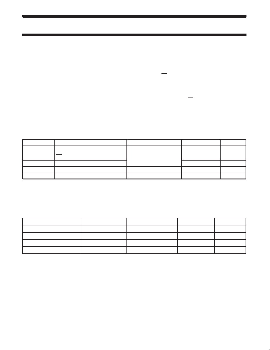
QUICK REFERENCE DATA
GND = 0V; Tamb = 25°C; tr =tf v2.5 ns
SYMBOL
PARAMETER
CONDITIONS
TYPICAL
UNIT
tPHL/tPLH
Propagation delay
CP to Qn;
MR to Qn
CL = 15pF
VCC = 3.3V
12
13
ns
fmax
Maximum clock frequency
110
MHz
CI
Input capacitance
3.5
pF
CPD
Power dissipation capacitance per flip-flop
Notes 1 and 2
20
pF
NOTES:
1. CPD is used to determine the dynamic power dissipation (PD in W)
PD = CPD
VCC2 x fi )S (CL
VCC2
fo) where:
fi = input frequency in MHz; CL = output load capacitance in pF;
fo = output frequency in MHz; VCC = supply voltage in V;
S (CL
VCC2
fo) = sum of the outputs.
2. The condition is VI = GND to VCC
ORDERING INFORMATION
PACKAGES
TEMPERATURE RANGE
OUTSIDE NORTH AMERICA
NORTH AMERICA
PKG. DWG. #
20-Pin Plastic DIL
–40
°C to +125°C
74LV273 N
SOT146-1
20-Pin Plastic SO
–40
°C to +125°C
74LV273 D
SOT163-1
20-Pin Plastic SSOP Type II
–40
°C to +125°C
74LV273 DB
SOT339-1
20-Pin Plastic TSSOP
–40
°C to +125°C
74LV273 PW
74LV273PW DH
SOT360-1
相关PDF资料 |
PDF描述 |
|---|---|
| 201M112-19G | ADAPTER SPIN COUPLING .491 DIA |
| 218M720D19B16 | ADPTR TINEL LOCK STR SHELL 20 |
| 218M720D19B12 | ADPTR TINEL LOCK STR SHELL 20 |
| 218M720D19B10 | ADPTR TINEL LOCK STR SHELL 20 |
| TXR54AB90-1408AI2 | ADPTR TINEL LOCK ANG SHELL 12,14 |
相关代理商/技术参数 |
参数描述 |
|---|---|
| 74LV273PWDH | 制造商:PHILIPS 制造商全称:NXP Semiconductors 功能描述:Octal D-type flip-flop with reset; positive-edge trigger |
| 74LV273PW-T | 功能描述:触发器 3.3V D-TYPE W/RESET POS RoHS:否 制造商:Texas Instruments 电路数量:2 逻辑系列:SN74 逻辑类型:D-Type Flip-Flop 极性:Inverting, Non-Inverting 输入类型:CMOS 输出类型: 传播延迟时间:4.4 ns 高电平输出电流:- 16 mA 低电平输出电流:16 mA 电源电压-最大:5.5 V 最大工作温度:+ 85 C 安装风格:SMD/SMT 封装 / 箱体:X2SON-8 封装:Reel |
| 74LV27D | 功能描述:逻辑门 TRIPLE 3-INPUT NOR GATE RoHS:否 制造商:Texas Instruments 产品:OR 逻辑系列:LVC 栅极数量:2 线路数量(输入/输出):2 / 1 高电平输出电流:- 16 mA 低电平输出电流:16 mA 传播延迟时间:3.8 ns 电源电压-最大:5.5 V 电源电压-最小:1.65 V 最大工作温度:+ 125 C 安装风格:SMD/SMT 封装 / 箱体:DCU-8 封装:Reel |
| 74LV27D,112 | 功能描述:逻辑门 TRIPLE 3-INPUT NOR RoHS:否 制造商:Texas Instruments 产品:OR 逻辑系列:LVC 栅极数量:2 线路数量(输入/输出):2 / 1 高电平输出电流:- 16 mA 低电平输出电流:16 mA 传播延迟时间:3.8 ns 电源电压-最大:5.5 V 电源电压-最小:1.65 V 最大工作温度:+ 125 C 安装风格:SMD/SMT 封装 / 箱体:DCU-8 封装:Reel |
| 74LV27D,118 | 功能描述:逻辑门 TRIPLE 3-INPUT NOR RoHS:否 制造商:Texas Instruments 产品:OR 逻辑系列:LVC 栅极数量:2 线路数量(输入/输出):2 / 1 高电平输出电流:- 16 mA 低电平输出电流:16 mA 传播延迟时间:3.8 ns 电源电压-最大:5.5 V 电源电压-最小:1.65 V 最大工作温度:+ 125 C 安装风格:SMD/SMT 封装 / 箱体:DCU-8 封装:Reel |
发布紧急采购,3分钟左右您将得到回复。