- 您现在的位置:买卖IC网 > PDF目录7974 > 74LVC574APW,112 (NXP Semiconductors)IC OCT D FF POS-EDG TRIG 20TSSOP PDF资料下载
参数资料
| 型号: | 74LVC574APW,112 |
| 厂商: | NXP Semiconductors |
| 文件页数: | 18/19页 |
| 文件大小: | 0K |
| 描述: | IC OCT D FF POS-EDG TRIG 20TSSOP |
| 产品培训模块: | Logic Packages |
| 标准包装: | 1,875 |
| 系列: | 74LVC |
| 功能: | 标准 |
| 类型: | D 型总线 |
| 输出类型: | 三态非反相 |
| 元件数: | 1 |
| 每个元件的位元数: | 8 |
| 延迟时间 - 传输: | 9ns |
| 触发器类型: | 正边沿 |
| 输出电流高,低: | 24mA,24mA |
| 电源电压: | 1.2 V ~ 3.6 V |
| 工作温度: | -40°C ~ 125°C |
| 安装类型: | 表面贴装 |
| 封装/外壳: | 20-TSSOP(0.173",4.40mm 宽) |
| 包装: | 管件 |
74LVC574A
All information provided in this document is subject to legal disclaimers.
NXP B.V. 2012. All rights reserved.
Product data sheet
Rev. 5 — 18 December 2012
8 of 19
NXP Semiconductors
74LVC574A
Octal D-type flip-flop; 5 V tolerance; positive edge-trigger; 3-state
[1]
Typical values are measured at Tamb =25 C and VCC = 1.2 V, 1.8 V, 2.5 V, 2.7 V and 3.3 V respectively.
[2]
tpd is the same as tPLH and tPHL.
ten is the same as tPZL and tPZH.
tdis is the same as tPLZ and tPHZ.
[3]
Skew between any two outputs of the same package switching in the same direction. This parameter is guaranteed by design.
[4]
CPD is used to determine the dynamic power dissipation (PD in W).
PD =CPD VCC2 fi N+ (CL VCC2 fo) where:
fi = input frequency in MHz; fo = output frequency in MHz
CL = output load capacitance in pF
VCC = supply voltage in Volts
N = number of inputs switching
(C
L VCC
2
f
o) = sum of the outputs
tW
pulse width
clock HIGH or LOW; see Figure 7
VCC = 1.65 V to 1.95 V
5.0
-
5.0
-
ns
VCC = 2.3 V to 2.7 V
4.0
-
4.0
-
ns
VCC = 2.7 V
3.3
-
3.3
-
ns
VCC = 3.0 V to 3.6 V
3.3
1.7
-
3.3
-
ns
tsu
set-up time
Dn to CP; see Figure 8
VCC = 1.65 V to 1.95 V
4.0
-
4.0
-
ns
VCC = 2.3 V to 2.7 V
2.5
-
2.5
-
ns
VCC = 2.7 V
2.0
-
2.0
-
ns
VCC = 3.0 V to 3.6 V
2.0
0.3
-
2.0
-
ns
th
hold time
Dn to CP; see Figure 8
VCC = 1.65 V to 1.95 V
3.0
-
3.0
-
ns
VCC = 2.3 V to 2.7 V
2.0
-
2.0
-
ns
VCC = 2.7 V
1.5
-
1.5
-
ns
VCC = 3.0 V to 3.6 V
+1.5
0.2
-
+1.5
-
ns
fmax
maximum
frequency
see Figure 7
VCC = 1.65 V to 1.95 V
100
-
80
-
MHz
VCC = 2.3 V to 2.7 V
125
-
100
-
MHz
VCC = 2.7 V
150
-
120
-
MHz
VCC = 3.0 V to 3.6 V
150
200
-
120
-
MHz
tsk(0)
output skew time
VCC = 3.0 V to 3.6 V
-
1.0
-
1.5
ns
CPD
power dissipation
capacitance
per flip-flop; VI = GND to VCC
VCC = 1.65 V to 1.95 V
-
11.2
-
pF
VCC = 2.3 V to 2.7 V
-
13.2
-
pF
VCC = 3.0 V to 3.6 V
-
14.9
-
pF
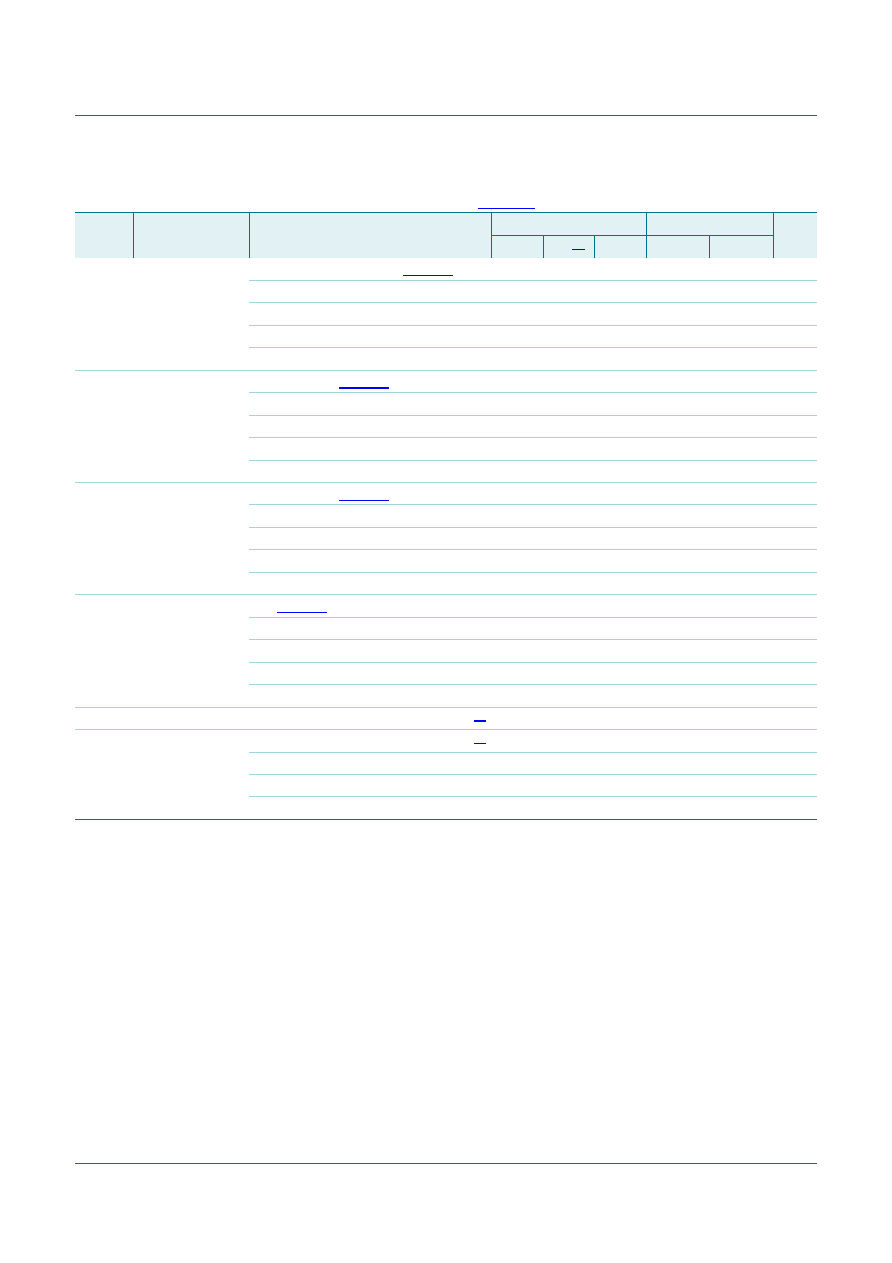
Table 7.
Dynamic characteristics …continued
Voltages are referenced to GND (ground = 0 V). For test circuit see Figure 10.
Symbol Parameter
Conditions
40 C to +85 C
40 C to +125 C Unit
Min
Typ[1]
Max
Min
Max
相关PDF资料 |
PDF描述 |
|---|---|
| MC10EL07DT | IC GATE XOR/XNOR ECL 2INP 8TSSOP |
| TXR54AB00-2207AI | ADPTR TINEL LOCK STR SHELL 22 |
| TXR54AB45-0804AI | ADPTR TINEL LOCK ANG SHELL 8 |
| 3314-5002 | PROTECT HEADER RT/ANG 14 CONTACT |
| TXR40AB00-0805BI | ADPTR TINEL LOCK STR SHELL 9, A |
相关代理商/技术参数 |
参数描述 |
|---|---|
| 74LVC574APW118 | 制造商:NXP Semiconductors 功能描述: |
| 74LVC574AQ20-13 | 功能描述:IC D-TYPE POS TRG SNGL 20QFN 制造商:diodes incorporated 系列:74LVC 包装:剪切带(CT) 零件状态:有效 功能:标准 类型:D 型 输出类型:非反相 元件数:1 每元件位数:8 频率 - 时钟:125MHz 不同 V,最大 CL 时的最大传播延迟:7.1ns @ 3.3V,30pF 触发器类型:正边沿 电流 - 输出高,低:24mA,24mA 电压 - 电源:1.65 V ~ 3.6 V 电流 - 静态:10μA 输入电容:4pF 工作温度:-40°C ~ 125°C(TA) 安装类型:表面贴装 封装/外壳:20-VFQFN 裸露焊盘 标准包装:1 |
| 74LVC574AT20-13 | 功能描述:IC D-TYPE POS TRG SNGL 20TSSOP 制造商:diodes incorporated 系列:74LVC 包装:剪切带(CT) 零件状态:有效 功能:标准 类型:D 型 输出类型:非反相 元件数:1 每元件位数:8 频率 - 时钟:125MHz 不同 V,最大 CL 时的最大传播延迟:7.1ns @ 3.3V,30pF 触发器类型:正边沿 电流 - 输出高,低:24mA,24mA 电压 - 电源:1.65 V ~ 3.6 V 电流 - 静态:10μA 输入电容:4pF 工作温度:-40°C ~ 125°C(TA) 安装类型:表面贴装 封装/外壳:20-TSSOP(0.173",4.40mm 宽) 标准包装:1 |
| 74LVC594ABQ | 制造商:NXP Semiconductors 功能描述:IC 8BIT SISO/PO SHIFT REG DH |
| 74LVC594ABQ,115 | 功能描述:计数器移位寄存器 3.3V SHIFT REG WITH RoHS:否 制造商:Texas Instruments 计数器类型: 计数顺序:Serial to Serial/Parallel 电路数量:1 封装 / 箱体:SOIC-20 Wide 逻辑系列: 逻辑类型: 输入线路数量:1 输出类型:Open Drain 传播延迟时间:650 ns 最大工作温度:+ 125 C 最小工作温度:- 40 C 封装:Reel |
发布紧急采购,3分钟左右您将得到回复。