- 您现在的位置:买卖IC网 > PDF目录7981 > 74LVC74APW,118 (NXP Semiconductors)IC DUAL D-TYPE FLIP-FLOP 14TSSOP PDF资料下载
参数资料
| 型号: | 74LVC74APW,118 |
| 厂商: | NXP Semiconductors |
| 文件页数: | 18/19页 |
| 文件大小: | 0K |
| 描述: | IC DUAL D-TYPE FLIP-FLOP 14TSSOP |
| 产品培训模块: | Logic Packages |
| 标准包装: | 2,500 |
| 系列: | 74LVC |
| 功能: | 设置(预设)和复位 |
| 类型: | D 型 |
| 输出类型: | 差分 |
| 元件数: | 2 |
| 每个元件的位元数: | 1 |
| 频率 - 时钟: | 250MHz |
| 延迟时间 - 传输: | 2.5ns |
| 触发器类型: | 正边沿 |
| 输出电流高,低: | 24mA,24mA |
| 电源电压: | 1.2 V ~ 3.6 V |
| 工作温度: | -40°C ~ 125°C |
| 安装类型: | 表面贴装 |
| 封装/外壳: | 14-TSSOP(0.173",4.40mm 宽) |
| 包装: | 带卷 (TR) |
74LVC74A
All information provided in this document is subject to legal disclaimers.
NXP B.V. 2012. All rights reserved.
Product data sheet
Rev. 7 — 20 November 2012
8 of 19
NXP Semiconductors
74LVC74A
Dual D-type flip-flop with set and reset; positive-edge trigger
[1]
Typical values are measured at Tamb =25 C and VCC = 1.2 V, 1.8 V, 2.5 V, 2.7 V and 3.3 V respectively.
[2]
tpd is the same as tPLH and tPHL.
[3]
Skew between any two outputs of the same package switching in the same direction. This parameter is guaranteed by design.
[4]
CPD is used to determine the dynamic power dissipation (PD in W).
PD =CPD VCC2 fi N+ (CL VCC2 fo) where:
fi = input frequency in MHz; fo = output frequency in MHz
CL = output load capacitance in pF
VCC = supply voltage in Volts
N = number of inputs switching
(C
L VCC
2
f
o) = sum of the outputs
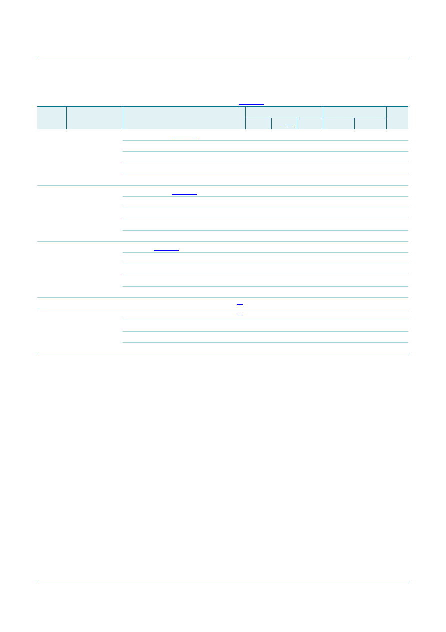
tsu
set-up time
nD to nCP; see Figure 7
VCC = 1.65 V to 1.95 V
3.0
-
3.0
-
ns
VCC = 2.3 V to 2.7 V
2.5
-
2.5
-
ns
VCC = 2.7 V
2.2
-
2.2
-
ns
VCC = 3.0 V to 3.6 V
2.0
0.8
-
2.0
-
ns
th
hold time
nD to nCP; see Figure 7
VCC = 1.65 V to 1.95 V
2.0
-
2.0
-
ns
VCC = 2.3 V to 2.7 V
1.5
-
1.5
-
ns
VCC = 2.7 V
1.0
-
1.0
-
ns
VCC = 3.0 V to 3.6 V
+1.0
0.2
-
1.0
-
ns
fmax
maximum
frequency
nCP; see Figure 7
VCC = 1.65 V to 1.95 V
100
-
80
-
MHz
VCC = 2.3 V to 2.7 V
125
-
100
-
MHz
VCC = 2.7 V
150
-
120
-
MHz
VCC = 3.0 V to 3.6 V
150
250
-
120
-
MHz
tsk(o)
output skew time VCC = 3.0 V to 3.6 V
-
1.0
-
1.5
ns
CPD
power
dissipation
capacitance
per flip-flop; VI =GND to VCC
VCC = 1.65 V to 1.95 V
-
12.4
-
pF
VCC = 2.3 V to 2.7 V
-
16.0
-
pF
VCC = 3.0 V to 3.6 V
-
19.1
-
pF
Table 8.
Dynamic characteristics …continued
Voltages are referenced to GND (ground = 0 V). For test circuit see Figure 9.
Symbol Parameter
Conditions
40 C to +85 C
40 C to +125 C Unit
Min
Typ[1]
Max
Min
Max
相关PDF资料 |
PDF描述 |
|---|---|
| TXR18AB00A2008AI | ADPTR TINEL LOCK STR SHELL 20 |
| TXR21AB00-2410AI | ADPTR TINEL LOCK STR SHELL 24 |
| TXR54AB00-1406BI | ADPTR TINEL LOCK STR SHELL 12,14 |
| TXR18AB00-1408AI | ADPTR TINEL LOCK STR SHELL 14 |
| SY100E404JC | IC GATE AND/NAND QUAD 28-PLCC |
相关代理商/技术参数 |
参数描述 |
|---|---|
| 74LVC74APW-Q100J | 制造商:NXP Semiconductors 功能描述:Flip Flop D-Type Pos-Edge 2-Element 14-Pin TSSOP T/R 制造商:NXP Semiconductors 功能描述:74LVC74APW-Q100/TSSOP14/REEL13 - Tape and Reel 制造商:NXP Semiconductors 功能描述:IC FLIP-FLOP DUAL D POS 14TSSOP |
| 74LVC74APWR | 制造商:Texas Instruments 功能描述:DUAL POSITIVE-EDGE-TRIGGERED D-TYPE FLIP-FLOPS WITH CLEAR AND PRESET LOW VOLTAG |
| 74LVC74APW-T | 制造商:NXP Semiconductors 功能描述:Flip Flop D-Type Pos-Edge 2-Element 14-Pin TSSOP T/R |
| 74LVC821ABQ | 制造商:NXP Semiconductors 功能描述:IC 10BIT D F-F TRI-ST DHVQF |
| 74LVC821ABQ,115 | 功能描述:触发器 10-BIT INTERFACE REG 3-ST RoHS:否 制造商:Texas Instruments 电路数量:2 逻辑系列:SN74 逻辑类型:D-Type Flip-Flop 极性:Inverting, Non-Inverting 输入类型:CMOS 输出类型: 传播延迟时间:4.4 ns 高电平输出电流:- 16 mA 低电平输出电流:16 mA 电源电压-最大:5.5 V 最大工作温度:+ 85 C 安装风格:SMD/SMT 封装 / 箱体:X2SON-8 封装:Reel |
发布紧急采购,3分钟左右您将得到回复。