- 您现在的位置:买卖IC网 > PDF目录2060 > 74LVX4245WMX (Fairchild Semiconductor)IC TXRX TRANSL DUAL 8BIT 24-SOIC PDF资料下载
参数资料
| 型号: | 74LVX4245WMX |
| 厂商: | Fairchild Semiconductor |
| 文件页数: | 5/8页 |
| 文件大小: | 0K |
| 描述: | IC TXRX TRANSL DUAL 8BIT 24-SOIC |
| 产品培训模块: | Logic Translator Solutions |
| 产品变化通告: | Product Discontinuation 27/Feb/2012 |
| 标准包装: | 1 |
| 系列: | 74LVX |
| 逻辑类型: | 收发器,非反相 |
| 元件数: | 1 |
| 每个元件的位元数: | 8 |
| 输出电流高,低: | 12mA,12mA; 24mA,24mA |
| 电源电压: | 2.7 V ~ 3.6 V,4.5 V ~ 5.5 V |
| 工作温度: | -40°C ~ 85°C |
| 安装类型: | 表面贴装 |
| 封装/外壳: | 24-SOIC(0.295",7.50mm 宽) |
| 供应商设备封装: | 24-SOIC |
| 包装: | 标准包装 |
| 产品目录页面: | 1212 (CN2011-ZH PDF) |
| 其它名称: | 74LVX4245WMXDKR |
5
www.fairchildsemi.com
74
L
V
X
4
24
5
Capacitance
Note 10: CPD is measured at 10 MHz
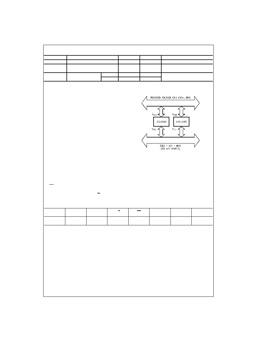
8-Bit Dual Supply Translating Transceiver
The LVX4245 is a dual supply device capable of bidirec-
tional signal translation. This level shifting ability provides
an efficient interface between low voltage CPU local bus
with memory and a standard bus defined by 5V I/O levels.
The device control inputs can be controlled by either the
low voltage CPU and core logic or a bus arbitrator with 5V
I/O levels.
Manufactured on a sub-micron CMOS process, the
LVX4245 is ideal for mixed voltage applications such as
notebook computers using 3.3V CPU’s and 5V peripheral
devices.
Power Up Considerations
To insure the system does not experience unnecessary ICC
current draw, bus contention, or oscillations during power
up, the following guidelines should be adhered to (refer to
Table 1):
Power up the control side of the device first. This is the
VCCA.
OE should ramp with or ahead of VCCA. This will help
guard against bus contention.
The Transmit/Receive control pin (T/R) should ramp with
or ahead of VCCA, this will ensure that the A Port data
pins are configured as inputs. With VCCA receiving
power first, the A I/O Port should be configured as inputs
to help guard against bus contention and oscillations.
A side data inputs should be driven to a valid logic level.
This will prevent excessive current draw.
The above steps will ensure that no bus contention or oscil-
lations, and therefore no excessive current draw occurs
during the power up cycling of these devices. These steps
will help prevent possible damage to the translator devices
and potential damage to other system components.
TABLE 1. Low Voltage Translator Power Up Sequencing Table
Please reference Application Note AN-5001 for more detailed information on using Fairchild’s LVX Low Voltage Dual
Supply CMOS Translating Transceivers.
Symbol
Parameter
Typ
Units
Conditions
CIN
Input Capacitance
4.5
pF
VCC = Open
CI/O
Input/Output
15
pF
VCCA = 5.0V
Capacitance
VCCB = 3.3V
CPD
Power Dissipation
B
→A55
pF
VCCA = 5.0V
Capacitance (Note 10)
A
→B40
pF
VCCB = 3.3V
Device Type
VCCA
VCCB
T/R
OE
A Side
I/O
B Side
I/O
Floatable Pin
Allowed
74LVX4245
5V
3V
ramp
logic
outputs
No
(power up 1st)
(power up 2nd)
with VCCA
0V or VCCA
相关PDF资料 |
PDF描述 |
|---|---|
| 74LVX541SJX | IC BUFF/DVR TRI-ST 8BIT 20SOP |
| 74LVX86SJX | IC GATE EXCL-OR QUAD 2IN 14SOP |
| 74LVXC4245MTCX | TXRX 8BIT DUAL CONF VOLT 24TSSOP |
| 74LVXC4245WMX | TXRX 8BIT DUAL CONF VOLT 24SOIC |
| 74VCX00BQX | IC GATE NAND QUAD 2IN LV 14DQFN |
相关代理商/技术参数 |
参数描述 |
|---|---|
| 74LVX4245WMX | 制造商:Fairchild Semiconductor Corporation 功能描述:Translator Logic IC |
| 74LVX541M | 功能描述:缓冲器和线路驱动器 Octal Buff/Line Drv RoHS:否 制造商:Micrel 输入线路数量:1 输出线路数量:2 极性:Non-Inverting 电源电压-最大:+/- 5.5 V 电源电压-最小:+/- 2.37 V 最大工作温度:+ 85 C 安装风格:SMD/SMT 封装 / 箱体:MSOP-8 封装:Reel |
| 74LVX541M_Q | 功能描述:缓冲器和线路驱动器 Octal Buff/Line Drv RoHS:否 制造商:Micrel 输入线路数量:1 输出线路数量:2 极性:Non-Inverting 电源电压-最大:+/- 5.5 V 电源电压-最小:+/- 2.37 V 最大工作温度:+ 85 C 安装风格:SMD/SMT 封装 / 箱体:MSOP-8 封装:Reel |
| 74LVX541MTC | 功能描述:缓冲器和线路驱动器 Octal Buff/Line Drv RoHS:否 制造商:Micrel 输入线路数量:1 输出线路数量:2 极性:Non-Inverting 电源电压-最大:+/- 5.5 V 电源电压-最小:+/- 2.37 V 最大工作温度:+ 85 C 安装风格:SMD/SMT 封装 / 箱体:MSOP-8 封装:Reel |
| 74LVX541MTCX | 功能描述:缓冲器和线路驱动器 Octal Buff/Line Drv RoHS:否 制造商:Micrel 输入线路数量:1 输出线路数量:2 极性:Non-Inverting 电源电压-最大:+/- 5.5 V 电源电压-最小:+/- 2.37 V 最大工作温度:+ 85 C 安装风格:SMD/SMT 封装 / 箱体:MSOP-8 封装:Reel |
发布紧急采购,3分钟左右您将得到回复。