- 您现在的位置:买卖IC网 > PDF目录8860 > 74LVXC3245QSCX (Fairchild Semiconductor)IC TRANSCEIVER 8BIT 24QSOP PDF资料下载
参数资料
| 型号: | 74LVXC3245QSCX |
| 厂商: | Fairchild Semiconductor |
| 文件页数: | 5/9页 |
| 文件大小: | 0K |
| 描述: | IC TRANSCEIVER 8BIT 24QSOP |
| 产品培训模块: | Logic Translator Solutions |
| 产品变化通告: | Mold Compound Change 12/Sept/2008 |
| 标准包装: | 2,500 |
| 系列: | 74LVXC |
| 逻辑功能: | 变换器,3 态 |
| 位数: | 8 |
| 输入类型: | TTL |
| 输出类型: | 逻辑 |
| 通道数: | 8 |
| 输出/通道数目: | 1 |
| 差分 - 输入:输出: | 无/无 |
| 传输延迟(最大): | 4.8ns |
| 电源电压: | 2.7 V ~ 3.6 V,3 V ~ 5.5 V |
| 工作温度: | -40°C ~ 85°C |
| 封装/外壳: | 24-SSOP(0.154",3.90mm 宽) |
| 供应商设备封装: | 24-QSOP |
| 包装: | 管件 |
LA4708N
No. A1783-5/9
Features of IC Inside and Usage Notes
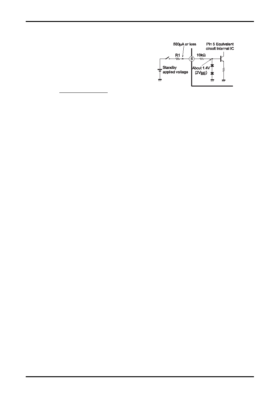
Standby function
Pin 5 is the standby switch pin. The amplifier is
turned on by applying approximately 2.5V or more
to this pin through an external resistor (R1).
If voltage in excess of 13.2V is to be applied to the
standby switch, calculate the value of R1 using the
following formula so that the current flowing into
pin 5 is 500
A or less:
R1 =
10k
Mute function
Pin 6 is the connector for the capacitor that determines the on time in order to prevent pop noise. By grounding this
pin, the amplifier can implement mute operation. In this case, the recovery time depends on C3.
How to reduce pop noise
Although the LA4708N reduces pop noise, an electrolytic capacitor of between 0.47 and 2.2F can be connected
between pin 8 and the pre-GND to further reduce pop noise that occurs when power supply is turned on/off
(standby switch on/off). The larger the capacitance, the lower the frequency of pop noise, and it is barely audible,
but sound residue of the sound signal is liable to linger when power is turned off. Pin 8 is the bias pin for the output
amplifier and normally is left open.
Protectors
In an output-to-ground and output-to-VCC short protector system configuration, if a DC resistor is connected
between amplifier output pin and GND, the protector may operate, causing the amplifier not to start operating.
Therefore, as a general rule, no DC resistor should be connected between amplifier output pin and GND.
In order to prevent damage or degradation which may be caused by abnormally heated IC, the LA4708N has a thermal
shutdown protector. Accordingly, if the IC junction temperature (Tj) climbs to around 170 to 180
C due to inadequate
heat dissipation, the thermal shutdown protector will operate to control the output gradually into attenuation.
Also be fully careful of handling other protectors built in the LA4708N.
Miscellaneous
Since pins 1 and 9, which are unused, are connected internally, they must be left open.
Pin 10 is an NC pin (no internal connection).
Applied voltage
1.4V
500
A
相关PDF资料 |
PDF描述 |
|---|---|
| MX7537JN+ | IC DAC 12BIT DL MULT 24-DIP |
| MAX542BESD+ | IC DAC 16BIT SER VOUT 5V 14-SOIC |
| D38999/20WD5AA | CONN HSG RCPT 5POS WALL MT PINS |
| MS27508E8F98PALC | CONN HSG RCPT 3POS BOX MNT PINS |
| VE-B2Z-MX-F3 | CONVERTER MOD DC/DC 2V 30W |
相关代理商/技术参数 |
参数描述 |
|---|---|
| 74LVXC3245QSCX-CUT TAPE | 制造商:FAIRCHILD 功能描述:74LVXC Series 3.6 V 8-Bit Dual Supply Configurable Voltage Interface Transceiver |
| 74LVXC3245TTR | 功能描述:总线收发器 Octal Bus Tansceiver RoHS:否 制造商:Fairchild Semiconductor 逻辑类型:CMOS 逻辑系列:74VCX 每芯片的通道数量:16 输入电平:CMOS 输出电平:CMOS 输出类型:3-State 高电平输出电流:- 24 mA 低电平输出电流:24 mA 传播延迟时间:6.2 ns 电源电压-最大:2.7 V, 3.6 V 电源电压-最小:1.65 V, 2.3 V 最大工作温度:+ 85 C 封装 / 箱体:TSSOP-48 封装:Reel |
| 74LVXC3245WM | 功能描述:总线收发器 8-Bit Dual Sup Trans RoHS:否 制造商:Fairchild Semiconductor 逻辑类型:CMOS 逻辑系列:74VCX 每芯片的通道数量:16 输入电平:CMOS 输出电平:CMOS 输出类型:3-State 高电平输出电流:- 24 mA 低电平输出电流:24 mA 传播延迟时间:6.2 ns 电源电压-最大:2.7 V, 3.6 V 电源电压-最小:1.65 V, 2.3 V 最大工作温度:+ 85 C 封装 / 箱体:TSSOP-48 封装:Reel |
| 74LVXC3245WM | 制造商:Fairchild Semiconductor Corporation 功能描述:IC 74LVXC SMD 74LVXC3245 SOIC24 |
| 74LVXC3245WM_Q | 功能描述:总线收发器 8-Bit Dual Sup Trans RoHS:否 制造商:Fairchild Semiconductor 逻辑类型:CMOS 逻辑系列:74VCX 每芯片的通道数量:16 输入电平:CMOS 输出电平:CMOS 输出类型:3-State 高电平输出电流:- 24 mA 低电平输出电流:24 mA 传播延迟时间:6.2 ns 电源电压-最大:2.7 V, 3.6 V 电源电压-最小:1.65 V, 2.3 V 最大工作温度:+ 85 C 封装 / 箱体:TSSOP-48 封装:Reel |
发布紧急采购,3分钟左右您将得到回复。