- 您现在的位置:买卖IC网 > PDF目录8063 > 74VCX245MTC (Fairchild Semiconductor)IC TRANSCVR BIDIRECT LV 20TSSOP PDF资料下载
参数资料
| 型号: | 74VCX245MTC |
| 厂商: | Fairchild Semiconductor |
| 文件页数: | 6/11页 |
| 文件大小: | 0K |
| 描述: | IC TRANSCVR BIDIRECT LV 20TSSOP |
| 标准包装: | 73 |
| 系列: | 74VCX |
| 逻辑类型: | 收发器,非反相 |
| 元件数: | 1 |
| 每个元件的位元数: | 8 |
| 输出电流高,低: | 24mA,24mA |
| 电源电压: | 1.4 V ~ 3.6 V |
| 工作温度: | -40°C ~ 85°C |
| 安装类型: | 表面贴装 |
| 封装/外壳: | 20-TSSOP(0.173",4.40mm 宽) |
| 供应商设备封装: | 20-TSSOP |
| 包装: | 管件 |
4
INDUSTRIAL TEMPERATURERANGE
IDT72V73260 3.3V TIME SLOT INTERCHANGE
DIGITAL SWITCH 16,384 x 16,384
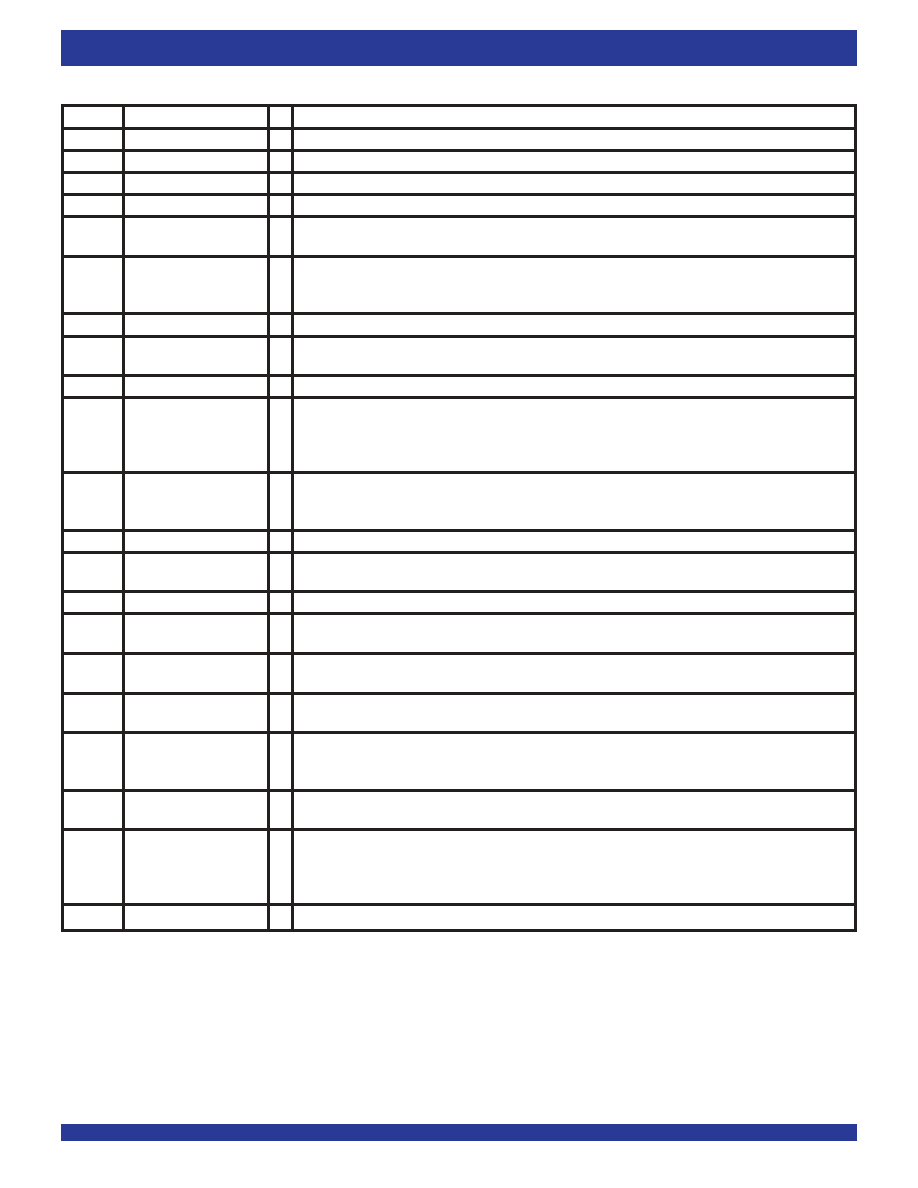
PIN DESCRIPTION
SYMBOL
NAME
I/O
DESCRIPTION
A0-15
Address 0 to 15
I
These address lines access all internal memories.
C32i
Clock
I
Serial clock for shifting data in/out on the serial data stream. This input accepts a 32.768 MHz clock.
CS
Chip Select
I
This active LOW input is used by a microprocessor to activate the microprocessor port of IDT72V73260.
D0-15
Data Bus 0-15
I/O
These pins are the data bits of the microprocessor port.
DS
Data Strobe
I
This active LOW input works in conjunction with
CS to enable the read and write operations and sets the
data bus lines (D0-D15).
DTA
Data Transfer
O
Indicates that a data bus transfer is complete. When the bus cycle ends, this pin drives HIGH and then goes
Acknowledgment
high-impedance, allowing for faster bus cycles with a weaker pull-up resistor. A pull-up resistor is required
to hold a HIGH level when the pin is in high-impedance.
FE
Frame Evaluation
I
This input can be used to measure delay in the data path by comparing the frame pulse, F32i, with this input.
F32i
Frame Pulse
I
This input accepts and automatically identifies frame synchronization signals formatted according to
ST-BUSand GCI specifications.
GND
Ground
Ground Rail
ODE
Output Drive Enable
I
This is the output enable control for the TX serial outputs. When the ODE input is LOW and the Output Stand
By bit of the Control Register is LOW, all TX outputs are in a high-impedance state. If this input is HIGH, the TX
output drivers are enabled. However, each channel may still be put into a high-impedance state by using the
per-channel control bits in the Connection Memory.
RESET
Device Reset
I
This input puts the IDT72V73260 into a reset state that clears the device internal counters, registers and
brings TX0-31 and D0-D15 into a high-impedance state. The
RESET pin must be held LOW for a minimum
of 20ns to properly reset the device.
R/
W
Read/Write
I
This input controls the direction of the data bus lines (D0-D15) during a microprocessor access.
RX0-31
DataStream
I
Serial data input stream. These streams have a data rate of 32.768Mb/s.
Input 0 to 31
TCK
Test Clock
I
Provides the clock to the JTAG test logic.
TDI
Test Serial Data In
I
JTAG serial test instructions and data are shifted in on this pin. This pin is pulled HIGH by an internal pull-up
when not driven.
TDO
Test Serial Data Out
O
JTAG serial data is output on this pin on the falling edge of TCK. This pin is held in high-impedance state
when JTAG scan is not enabled.
TMS
Test Mode Select
I
JTAG signal that controls the state transitions of the TAP controller. This pin is pulled HIGH by an internal
pull-up when not driven.
TRST
TestReset
I
Asynchronously initializes the JTAG TAP controller by putting it in the Test-Logic-Reset state. This pin is
pulled by an internal pull-up when not driven. This pin should be pulsed LOW on power-up, or held LOW,
to ensure that the IDT72V73260 is in the normal functional mode.
TX0-15
TX Output 0 to 15
O
Serial data output stream. These streams have a data rate of 32.768Mb/s.
(Three-StateOutputs)
TX16-31/ TX Output 16 to 31/
O
When all 32 output streams are selected via Control Register, these pins are the output streams TX16 to TX31
OEI0-15
OutputEnable
and operate at 32.768Mb/s. When output enable function is selected, these pins reflect the active or
Indication 0 to 15
high-impedance status for the corresponding output stream Output Enable Indication0-15.
(Three-StateOutputs)
VCC
+3.3 Volt Power Supply.
相关PDF资料 |
PDF描述 |
|---|---|
| MC74HC367ADG | IC BUFFER 3ST HEX 16-SOIC |
| 20IMX4-03-8 | CONVERT 4W 3V DC/DC |
| OSTTS15515A | TERM BLOCK PLUG 5.08MM 15POS |
| 20IMX4-0505-8 | CONVERT 4W 2X 5V DC/DC |
| 74HC161PW,118 | IC SYNC 4BIT BINAR COUNT 16TSSOP |
相关代理商/技术参数 |
参数描述 |
|---|---|
| 74VCX245MTCX | 功能描述:总线收发器 Bidir Transceiver RoHS:否 制造商:Fairchild Semiconductor 逻辑类型:CMOS 逻辑系列:74VCX 每芯片的通道数量:16 输入电平:CMOS 输出电平:CMOS 输出类型:3-State 高电平输出电流:- 24 mA 低电平输出电流:24 mA 传播延迟时间:6.2 ns 电源电压-最大:2.7 V, 3.6 V 电源电压-最小:1.65 V, 2.3 V 最大工作温度:+ 85 C 封装 / 箱体:TSSOP-48 封装:Reel |
| 74VCX245WM | 功能描述:总线收发器 Bidir Transceiver RoHS:否 制造商:Fairchild Semiconductor 逻辑类型:CMOS 逻辑系列:74VCX 每芯片的通道数量:16 输入电平:CMOS 输出电平:CMOS 输出类型:3-State 高电平输出电流:- 24 mA 低电平输出电流:24 mA 传播延迟时间:6.2 ns 电源电压-最大:2.7 V, 3.6 V 电源电压-最小:1.65 V, 2.3 V 最大工作温度:+ 85 C 封装 / 箱体:TSSOP-48 封装:Reel |
| 74VCX245WM_Q | 功能描述:总线收发器 Bidir Transceiver RoHS:否 制造商:Fairchild Semiconductor 逻辑类型:CMOS 逻辑系列:74VCX 每芯片的通道数量:16 输入电平:CMOS 输出电平:CMOS 输出类型:3-State 高电平输出电流:- 24 mA 低电平输出电流:24 mA 传播延迟时间:6.2 ns 电源电压-最大:2.7 V, 3.6 V 电源电压-最小:1.65 V, 2.3 V 最大工作温度:+ 85 C 封装 / 箱体:TSSOP-48 封装:Reel |
| 74VCX245WMX | 功能描述:总线收发器 Bidir Transceiver RoHS:否 制造商:Fairchild Semiconductor 逻辑类型:CMOS 逻辑系列:74VCX 每芯片的通道数量:16 输入电平:CMOS 输出电平:CMOS 输出类型:3-State 高电平输出电流:- 24 mA 低电平输出电流:24 mA 传播延迟时间:6.2 ns 电源电压-最大:2.7 V, 3.6 V 电源电压-最小:1.65 V, 2.3 V 最大工作温度:+ 85 C 封装 / 箱体:TSSOP-48 封装:Reel |
| 74VCX32 | 制造商:FAIRCHILD 制造商全称:Fairchild Semiconductor 功能描述:Low Voltage Quad 2-Input OR Gate with 3.6V Tolerant Inputs and Outputs |
发布紧急采购,3分钟左右您将得到回复。