- 您现在的位置:买卖IC网 > PDF目录370133 > 74VHC4046M (FAIRCHILD SEMICONDUCTOR CORP) CMOS Phase Lock Loop PDF资料下载
参数资料
| 型号: | 74VHC4046M |
| 厂商: | FAIRCHILD SEMICONDUCTOR CORP |
| 元件分类: | XO, clock |
| 英文描述: | CMOS Phase Lock Loop |
| 中文描述: | PHASE LOCKED LOOP, 12 MHz, PDSO16 |
| 封装: | 0.150 INCH, MS-012, SOIC-16 |
| 文件页数: | 9/14页 |
| 文件大小: | 283K |
| 代理商: | 74VHC4046M |
Detailed Circuit Description
(Continued)
the capacitor once the capacitor charges up to the thresh-
old of the schmitt trigger the oscillator logic flips the capaci-
tor over and causes the mirror to charge the opposite side
of the capacitor. The output from the internal logic is then
taken to pin 4.
The input to the VCO is a very high impedance CMOS input
and so it will not load down the loop filter, easing the filters
design. In order to make signals at the VCO input accessible
without degrading the loop performance a source follower
transistor is provided. This transistor can be used by con-
necting a resistor to ground and its drain output will follow
the VCO input signal.
An inhibit signal is provided to allow disabling of the VCO
and the source follower. This is useful if the internal VCO is
not being used. A logic high on inhibit disables the VCO and
source follower.
The output of the VCO is a standard high speed CMOS
output with an equivalent LSTTL fanout of 10. The VCO
output is approximately a square wave. This output can ei-
ther directly feed the comparator input of the phase compar-
ators or feed external prescalers (counters) to enable fre-
quency synthesis.
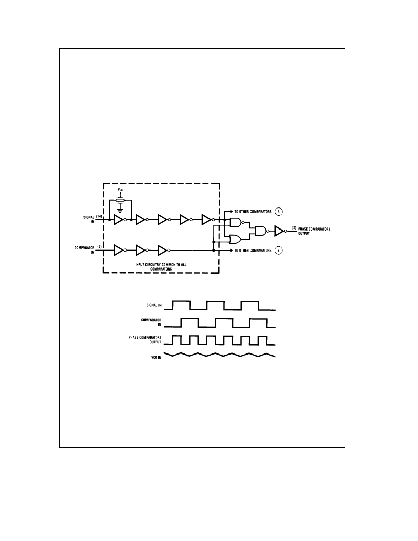
PHASE COMPARATORS
All three phase comparators share two inputs, Signal In and
Comparator In. The Signal In has a special DC bias network
that enables AC coupling of input signals. If the signals are
not AC coupled then this input requires logic levels the
same as standard 74VHC. The Comparator input is a stan-
dard digital input. Both input structures are shown in Figure
3.
The outputs of these comparators are essentially standard
74VHC voltage outputs. (Comparator II is TRI-STATE.)
TL/F/11675-19
FIGURE 3. Logic Diagram for Phase Comparator I and the Common Input Circuit for All Three Comparators
TL/F/11675–20
FIGURE 4. Typical Phase Comparator I. Waveforms
9
相关PDF资料 |
PDF描述 |
|---|---|
| 74VHC4046N | 3-Line To 8-Line Decoders/Demultiplexers 16-TSSOP -40 to 85 |
| 74VHC4046MTCX | Code Hopping Encoder 3.5- 13V, -40C to +85C, 8-SOIC 150mil, T/R |
| 74VHC4052 | Analog Multiplexers/Demultiplexers |
| 74VHC4052 | 8-Channel Analog Multiplexer . Dual 4-Channel Analog Multiplexer . Triple 2-Channel Analog Multiplexer |
| 74VHC4052M | 8-Channel Analog Multiplexer . Dual 4-Channel Analog Multiplexer . Triple 2-Channel Analog Multiplexer |
相关代理商/技术参数 |
参数描述 |
|---|---|
| 74VHC4046M | 制造商:Fairchild Semiconductor Corporation 功能描述:IC 74VHC CMOS SMD 74VHC4046 |
| 74VHC4046M_Q | 功能描述:锁相环 - PLL CMOS Phase-Lock Loop RoHS:否 制造商:Silicon Labs 类型:PLL Clock Multiplier 电路数量:1 最大输入频率:710 MHz 最小输入频率:0.002 MHz 输出频率范围:0.002 MHz to 808 MHz 电源电压-最大:3.63 V 电源电压-最小:1.71 V 最大工作温度:+ 85 C 最小工作温度:- 40 C 封装 / 箱体:QFN-36 封装:Tray |
| 74VHC4046MTC | 功能描述:锁相环 - PLL CMOS Phase-Lock Loop RoHS:否 制造商:Silicon Labs 类型:PLL Clock Multiplier 电路数量:1 最大输入频率:710 MHz 最小输入频率:0.002 MHz 输出频率范围:0.002 MHz to 808 MHz 电源电压-最大:3.63 V 电源电压-最小:1.71 V 最大工作温度:+ 85 C 最小工作温度:- 40 C 封装 / 箱体:QFN-36 封装:Tray |
| 74VHC4046MTCX | 功能描述:锁相环 - PLL CMOS Phase-Lock Loop RoHS:否 制造商:Silicon Labs 类型:PLL Clock Multiplier 电路数量:1 最大输入频率:710 MHz 最小输入频率:0.002 MHz 输出频率范围:0.002 MHz to 808 MHz 电源电压-最大:3.63 V 电源电压-最小:1.71 V 最大工作温度:+ 85 C 最小工作温度:- 40 C 封装 / 箱体:QFN-36 封装:Tray |
| 74VHC4046MTCX_NL | 功能描述:锁相环 - PLL FINISHED GOOD RoHS:否 制造商:Silicon Labs 类型:PLL Clock Multiplier 电路数量:1 最大输入频率:710 MHz 最小输入频率:0.002 MHz 输出频率范围:0.002 MHz to 808 MHz 电源电压-最大:3.63 V 电源电压-最小:1.71 V 最大工作温度:+ 85 C 最小工作温度:- 40 C 封装 / 箱体:QFN-36 封装:Tray |
发布紧急采购,3分钟左右您将得到回复。