- 您现在的位置:买卖IC网 > PDF目录370133 > 74VHC4052 (ON SEMICONDUCTOR) Analog Multiplexers/Demultiplexers PDF资料下载
参数资料
| 型号: | 74VHC4052 |
| 厂商: | ON SEMICONDUCTOR |
| 英文描述: | Analog Multiplexers/Demultiplexers |
| 中文描述: | 模拟多路复用器/解复用器 |
| 文件页数: | 11/16页 |
| 文件大小: | 341K |
| 代理商: | 74VHC4052 |
MC74VHC4051, MC74VHC4052, MC74VHC4053
http://onsemi.com
11
RL
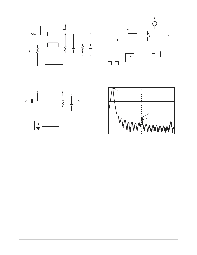
Figure 11. Crosstalk Between Any Two
Switches, Test Set–Up
Figure 12. Power Dissipation Capacitance,
Test Set–Up
Figure 14a. Total Harmonic Distortion, Test Set–Up
Figure 13b. Plot, Harmonic Distortion
0
–10
–20
–30
–40
–50
–100
1.0
2.0
3.125
FREQUENCY (kHz)
d
–60
–70
–80
–90
FUNDAMENTAL FREQUENCY
DEVICE
SOURCE
ON
6
7
8
16
VEE
CL*
*Includes all probe and jig capacitance
OFF
RL
RL
VIS
RL
CL*
VOS
fin
0.1
μ
F
ON/OFF
6
7
8
16
VCC
CHANNEL SELECT
NC
COMMON O/I
OFF/ON
ANALOG I/O
VCC
A
11
VCC
VEE
ON
6
7
8
16
VCC
VEE
0.1
μ
F
CL*
fin
RL
TO
DISTORTION
METER
*Includes all probe and jig capacitance
VOS
VIS
APPLICATIONS INFORMATION
The Channel Select and Enable control pins should be at
VCC or GND logic levels. VCC being recognized as a logic
high and GND being recognized as a logic low. In this
example:
VCC = +5V = logic high
GND = 0V = logic low
The maximum analog voltage swings are determined by
the supply voltages VCC and VEE. The positive peak analog
voltage should not exceed VCC. Similarly, the negative peak
analog voltage should not go below VEE. In this example,
the difference between VCC and VEE is ten volts. Therefore,
using the configuration of Figure 15, a maximum analog
signal of ten volts peak–to–peak can be controlled. Unused
analog inputs/outputs may be left floating (i.e., not
connected). However, tying unused analog inputs and
outputs to VCC or GND through a low value resistor helps
minimize crosstalk and feedthrough noise that may be
picked up by an unused switch.
Although used here, balanced supplies are not a
requirement. The only constraints on the power supplies are
that:
VCC – GND = 2 to 6 volts
VEE – GND = 0 to –6 volts
VCC – VEE = 2 to 12 volts
and VEE
≤
GND
When voltage transients above VCC and/or below VEE are
anticipated on the analog channels, external Germanium or
Schottky diodes (Dx) are recommended as shown in Figure
16. These diodes should be able to absorb the maximum
anticipated current surges during clipping.
相关PDF资料 |
PDF描述 |
|---|---|
| 74VHC4052 | 8-Channel Analog Multiplexer . Dual 4-Channel Analog Multiplexer . Triple 2-Channel Analog Multiplexer |
| 74VHC4052M | 8-Channel Analog Multiplexer . Dual 4-Channel Analog Multiplexer . Triple 2-Channel Analog Multiplexer |
| 74VHC4052MTC | 8-Channel Analog Multiplexer . Dual 4-Channel Analog Multiplexer . Triple 2-Channel Analog Multiplexer |
| 74VHC4052N | Dual 2-Line To 4-Line Decoders/Demultiplexers 16-SOIC -40 to 85 |
| 74VHC4052WM | 8-Channel Analog Multiplexer . Dual 4-Channel Analog Multiplexer . Triple 2-Channel Analog Multiplexer |
相关代理商/技术参数 |
参数描述 |
|---|---|
| 74VHC4052AFT | 功能描述:2 Circuit IC Switch 4:1 37 Ohm 16-TSSOPB 制造商:toshiba semiconductor and storage 系列:- 包装:剪切带(CT) 零件状态:有效 开关电路:SP4T 多路复用器/解复用器电路:4:1 电路数:2 导通电阻(最大值):37 欧姆 通道至通道匹配(ΔRon):5 欧姆 电压 -?电源,单(V+):2 V ~ 5.5 V 电压 - 电源,双(V±):- 开关时间(Ton, Tof)(最大值):12ns,12ns -3db 带宽:230MHz 电荷注入:- 沟道电容 (CS(off),CD(off)):0.5pF,13.1pF 电流 - 漏泄(IS(off))(最大值):100nA 串扰:-45dB @ 1MHz 工作温度:-40°C ~ 85°C(TA) 封装/外壳:16-TSSOP(0.173",4.40mm 宽) 供应商器件封装:16-TSSOPB 标准包装:1 |
| 74VHC4052AFT(BJ) | 功能描述:X34 PB-F VHS TSSOP 14 CMOS LOGIC 制造商:toshiba semiconductor and storage 系列:* 包装:剪切带(CT) 零件状态:在售 封装/外壳:16-TSSOP(0.173",4.40mm 宽) 供应商器件封装:16-TSSOPB 标准包装:1 |
| 74VHC4052M | 功能描述:多路器开关 IC Dl 4-Chan Ana Multi RoHS:否 制造商:Texas Instruments 通道数量:1 开关数量:4 开启电阻(最大值):7 Ohms 开启时间(最大值): 关闭时间(最大值): 传播延迟时间:0.25 ns 工作电源电压:2.3 V to 3.6 V 工作电源电流: 最大工作温度:+ 85 C 安装风格:SMD/SMT 封装 / 箱体:UQFN-16 |
| 74VHC4052M | 制造商:Fairchild Semiconductor Corporation 功能描述:IC 74VHC CMOS SMD 74VHC4052 |
| 74VHC4052M_Q | 功能描述:多路器开关 IC Dl 4-Chan Ana Multi RoHS:否 制造商:Texas Instruments 通道数量:1 开关数量:4 开启电阻(最大值):7 Ohms 开启时间(最大值): 关闭时间(最大值): 传播延迟时间:0.25 ns 工作电源电压:2.3 V to 3.6 V 工作电源电流: 最大工作温度:+ 85 C 安装风格:SMD/SMT 封装 / 箱体:UQFN-16 |
发布紧急采购,3分钟左右您将得到回复。