- 您现在的位置:买卖IC网 > PDF目录369340 > 75232-R20-R (UNISONIC TECHNOLOGIES CO LTD) 5V High-Speed RS-232 Transceivers with 0.1uF Capacitors PDF资料下载
参数资料
| 型号: | 75232-R20-R |
| 厂商: | UNISONIC TECHNOLOGIES CO LTD |
| 元件分类: | 通用总线功能 |
| 英文描述: | 5V High-Speed RS-232 Transceivers with 0.1uF Capacitors |
| 中文描述: | TRIPLE LINE TRANSCEIVER, PDSO20 |
| 封装: | 0.209 INCH, SSOP-20 |
| 文件页数: | 3/10页 |
| 文件大小: | 310K |
| 代理商: | 75232-R20-R |
75232
LINEAR INTEGRATED CIRCUIT
UNISONIC TECHNOLOGIES CO., LTD
www.unisonic.com.tw
QW-R113-005,D
3 of 10
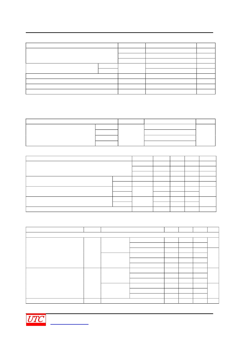
ABS OLUT E MAX IMUM RAT INGS
PARAMETER
SYMBOL
V
DD
V
SS
V
CC
RATINGS
15
-15
10
-15
~
7
-30
~
30
-15
~
15
20
0 ~ +70
-40 ~ +150
UNIT
V
V
V
V
V
V
mA
°
C
°
C
Supply Voltage (Note 2)
Driver
Receiver
Input Voltage Range
V
IN
Driver Output Voltage Range
Receiver Low Level Output Current
Operation Temperature
Storage Temperature
Note: 1.Absolute maximum ratings are those values beyond which the device could be permanently damaged.
Absolute maximum ratings are stress ratings only and functional device operation is not implied.
2. All voltages are with respect to the network ground terminal.
V
OUT
I
OUT
T
OPR
T
STG
T HERMAL DATA
PARAMETER
SYMBOL
RATINGS
70
100
115
115
UNIT
DIP-20
SOP-20
SSOP-20
TSSOP-20
Thermal Resistance Junction- Ambient
θ
JA
°
C/W
RECOMMENDED OPERAT ING
RAT INGS
PARAMETER
SYMBOL
V
DD
V
SS
V
CC
V
IH
V
IL
MIN
7.5
-7.5
4.5
1.9
0
TYP
9
-9
5
MAX
15
-15
5.5
0.8
-6.0
-0.5
6
16
70
UNIT
V
V
V
V
V
Supply Voltage
High
Low
Driver
Receiver
Driver
Receiver
Level Input Voltage (driver only)
High Level Output Current
I
OH
mA
Low Level Output Current
I
OL
mA
Operating Free-air Temperature
T
OPR
°
C
E LECT RICAL CHARACT ERIST ICS
(Over recommended supply voltage and operating temperature ranges, unless otherwise specified)
PARAMETER
SYMBOL
TEST CONDITIONS
MIN
TYP
MAX
UNIT
SUPPLY CURRENTS
V
DD
=9V, V
SS
=-9V
V
DD
=12, V
SS
=-12V
15
19
25
4.5
5.5
9
-15
-19
-25
-3.2
-3.2
-3.2
30
mA
No load.
All inputs at 1.9VV
DD
=15, V
SS
=-15V
V
DD
=9V, V
SS
=-9V
V
DD
=12, V
SS
=-12V
All inputs at 0.8VV
DD
=15, V
SS
=-15V
V
DD
=9V, V
SS
=-9V
V
DD
=12, V
SS
=-12V
All inputs at 1.9VV
DD
=15, V
SS
=-15V
V
DD
=9V, V
SS
=-9V
V
DD
=12, V
SS
=-12V
All inputs at 0.8VV
DD
=15, V
SS
=-15V
No load. All inputs at 5V, V
CC
=5V
Supply Current from V
DD
I
DD
No load.
mA
No load.
mA
Supply Current from V
SS
I
SS
No load.
mA
Supply Current from V
CC
I
CC
mA
相关PDF资料 |
PDF描述 |
|---|---|
| 75232-R20-T | 5V High-Speed RS-232 Transceivers with 0.1uF Capacitors |
| 75232-S20-R | 5V High-Speed RS-232 Transceivers with 0.1uF Capacitors |
| 75232 | 5V High-Speed RS-232 Transceivers with 0.1uF Capacitors |
| 75232 | Line Driver / Receiver |
| 7525 | X-ray Thickness Gage |
相关代理商/技术参数 |
参数描述 |
|---|---|
| 75232-R20-T | 制造商:UTC-IC 制造商全称:UTC-IC 功能描述:MULTIPLE RS-232 DRIVERS AND RECEIVERS |
| 75232-S20-R | 制造商:UTC-IC 制造商全称:UTC-IC 功能描述:MULTIPLE RS-232 DRIVERS AND RECEIVERS |
| 75232-S20-T | 制造商:UTC-IC 制造商全称:UTC-IC 功能描述:MULTIPLE RS-232 DRIVERS AND RECEIVERS |
| 752335-000 | 制造商:TE Connectivity 功能描述:55A1812-16-9-9CS2275 - Bulk |
| 7523362001 | 制造商:TE Connectivity 功能描述:NYLON-3/16-X-STK |
发布紧急采购,3分钟左右您将得到回复。