- 您现在的位置:买卖IC网 > PDF目录370133 > 7534 (Renesas Technology Corp.) SINGLE-CHIP 8-BIT CMOS MICROCOMPUTER PDF资料下载
参数资料
| 型号: | 7534 |
| 厂商: | Renesas Technology Corp. |
| 英文描述: | SINGLE-CHIP 8-BIT CMOS MICROCOMPUTER |
| 中文描述: | 单芯片8位CMOS微机 |
| 文件页数: | 44/55页 |
| 文件大小: | 610K |
| 代理商: | 7534 |
第1页第2页第3页第4页第5页第6页第7页第8页第9页第10页第11页第12页第13页第14页第15页第16页第17页第18页第19页第20页第21页第22页第23页第24页第25页第26页第27页第28页第29页第30页第31页第32页第33页第34页第35页第36页第37页第38页第39页第40页第41页第42页第43页当前第44页第45页第46页第47页第48页第49页第50页第51页第52页第53页第54页第55页
7534 Group
Rev.2.00 Jun 21, 2004 page 44 of 54
REJ03B0099-0200Z
Timing Requirements
Table 12 Timing requirements (V
CC
= 4.1 to 5.5 V, V
SS
= 0 V, Ta = –20 to 85 °C, unless otherwise noted)
Min.
15
166
70
70
200
80
80
1000
400
400
200
200
Typ.
Max.
Symbol
Parameter
Limits
Unit
t
W
(RESET)
t
C
(X
IN
)
t
WH
(X
IN
)
t
WL
(X
IN
)
t
C
(CNTR)
t
WH
(CNTR)
t
WL
(CNTR)
t
C
(S
CLK
)
t
WH
(S
CLK
)
t
WL
(S
CLK
)
t
su
(S
DATA
–S
CLK
)
t
h
(S
CLK
–S
DATA
)
Reset input “L” pulse width
External clock input cycle time
External clock input “H” pulse width
External clock input “L” pulse width
CNTR
0
input cycle time
CNTR
0
, INT
0
, INT
1
input “H” pulse width
CNTR
0
, INT
0
, INT
1
input “L” pulse width
Serial I/O2 clock input cycle time
Serial I/O2 clock input “H” pulse width
Serial I/O2 clock input “L” pulse width
Serial I/O2 input set up time
Serial I/O2 input hold time
μs
ns
ns
ns
ns
ns
ns
ns
ns
ns
ns
ns
Switching Characteristics
Table 13 Switching characteristics (V
CC
= 4.1 to 5.5 V, V
SS
= 0 V, Ta = –20 to 85 °C, unless otherwise noted)
Min.
Typ.
Max.
Symbol
Parameter
Limits
Unit
t
WH
(S
CLK
)
t
WL
(S
CLK
)
t
d
(S
CLK
–S
DATA
)
t
v
(S
CLK
–S
DATA
)
t
r
(S
CLK
)
t
f
(S
CLK
)
t
r
(CMOS)
t
f
(CMOS)
t
r
(D+), t
r
(D-)
t
f
(D+), t
f
(D-)
Serial I/O2 clock output “H” pulse width
Serial I/O2 clock output “L” pulse width
Serial I/O2 output delay time
Serial I/O2 output valid time
Serial I/O2 clock output rising time
Serial I/O2 clock output falling time
CMOS output rising time (Note)
CMOS output falling time (Note)
USB output rising time, C
L
= 200 to 450 pF, Ta = 0 to 70 °C, V
CC
=
4.4 to 5.25 V
USB output falling time, C
L
= 200 to 450 pF, Ta = 0 to 70 °C, V
CC
=
4.4 to 5.25 V
Notes:
X
OUT
pin is excluded.
10
10
150
150
75
75
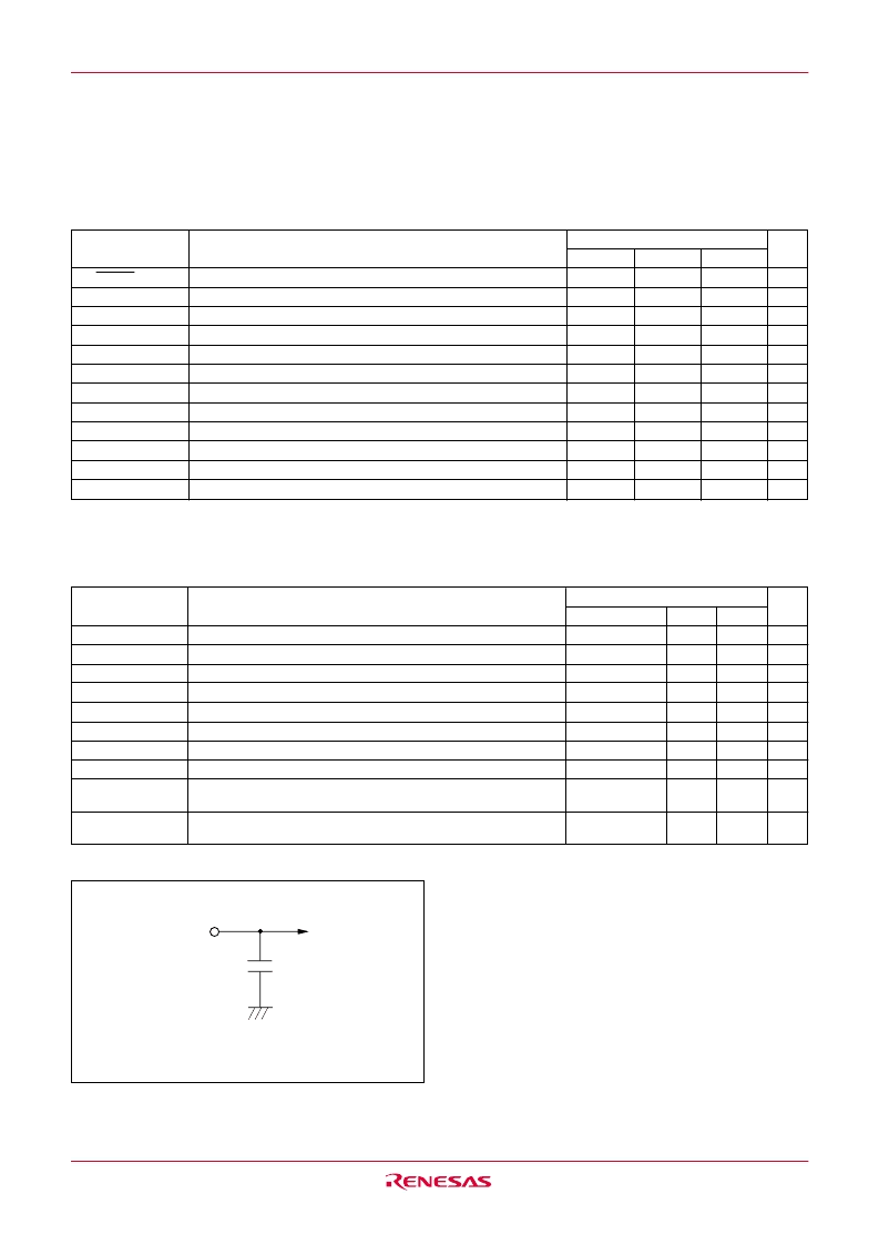
Fig. 49 Output switching characteristics measurement circuit
100 pF
Measured
output pin
CMOS output
t
C
(S
CLK
)/2–30
t
C
(S
CLK
)/2–30
0
ns
ns
ns
ns
ns
ns
ns
ns
ns
ns
140
30
30
30
30
300
300
相关PDF资料 |
PDF描述 |
|---|---|
| 7548 | SINGLE-CHIP 8-BIT CMOS MICROCOMPUTER |
| 7549 | SINGLE-CHIP 8-BIT CMOS MICROCOMPUTER |
| 75HQ | SCHOTTKY RECTIFIER |
| 75HQ030 | SCHOTTKY RECTIFIER |
| 75HQ035 | SCHOTTKY RECTIFIER |
相关代理商/技术参数 |
参数描述 |
|---|---|
| 7534_06 | 制造商:RENESAS 制造商全称:Renesas Technology Corp 功能描述:8-BIT SINGLE-CHIP MICROCOMPUTER |
| 75340 | 功能描述:BIT MICRO HEX SYST4 4.0MM 28MM RoHS:否 类别:工具 >> 螺钉和螺母驱动器 - 刀片和位 系列:系统 4 标准包装:1 系列:TorqueVario™ 类型:十字槽刀片 尺寸:#2 长度:7.48"(190mm) 特点:绝缘达 10,000V 重量:0.07 磅(31.75g) |
| 753-40.4M-A | 制造商:OSCILENT 制造商全称:Oscilent Corporation 功能描述:Ceramic Trap For TV/VCR |
| 753-40.7M-A | 制造商:OSCILENT 制造商全称:Oscilent Corporation 功能描述:Ceramic Trap For TV/VCR |
| 753-402 | 制造商:WAGO Innovative Connections 功能描述:4DI 24V DC 3,0ms |
发布紧急采购,3分钟左右您将得到回复。