参数资料
| 型号: | 78M6613-SP-1 |
| 厂商: | Maxim Integrated Products |
| 文件页数: | 6/33页 |
| 文件大小: | 0K |
| 描述: | EVAL KIT 78M6613-SP-1 |
| 标准包装: | 1 |
| 系列: | * |
第1页第2页第3页第4页第5页当前第6页第7页第8页第9页第10页第11页第12页第13页第14页第15页第16页第17页第18页第19页第20页第21页第22页第23页第24页第25页第26页第27页第28页第29页第30页第31页第32页第33页
�� �
�
�78M6613� Data� Sheet�
�DS_6613_018�
�1.2�
�Analog� Front� End� (AFE)�
�The� AFE� of� the� 78M6613� is� comprised� of� an� input� multiplexer,� a� delta-sigma� A/D� converter� and� a�
�voltage� reference.�
�1.2.1�
�Input� Multiplexer�
�The� input� multiplexer� supports� up� to� four� input� signals� that� are� applied� to� pins� A0,� A1,� A2� and� A3� of� the�
�device.� Additionally,� using� the� alternate� mux� selection,� it� has� the� ability� to� select� the� on-chip�
�temperature� sensor.� The� multiplexer� can� be� operated� in� two� modes:�
�?�
�?�
�During� a� normal� multiplexer� cycle,� the� signals� from� the� A0,� A2,� A1,� and� A3� pins� are� selected.�
�During� the� alternate� multiplexer� cycle,� the� temperature� signal� (TEMP)� is� selected,� along� with� the�
��The� alternate� mux� cycles� are� usually� performed� infrequently� (e.g.� every� second)� by� the� MPU.� Table� 1�
�details� the� regular� and� alternative� MUX� sequences.� Missing� samples� due� to� an� ALT� multiplexer�
�sequence� are� filled� in� by� the� CE.�
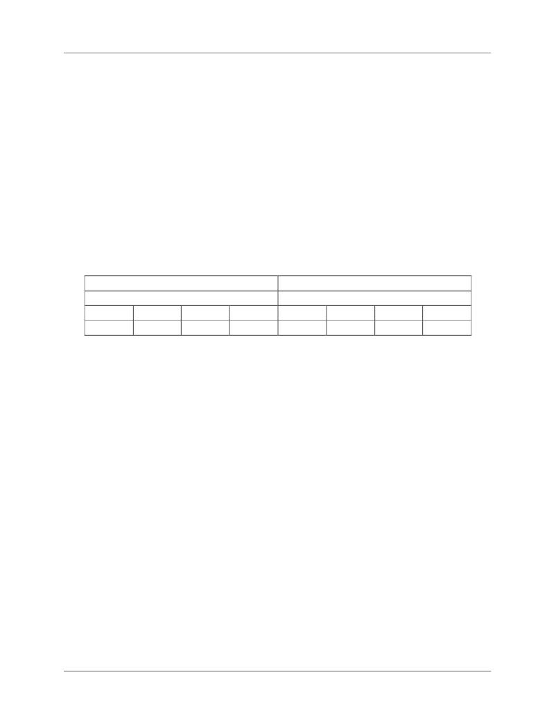
�Table� 1:� Inputs� Selected� in� Regular� and� Alternate� Multiplexer� Cycles�
�Regular� MUX� Sequence�
�Mux� State�
�ALT� MUX� Sequence�
�Mux� State�
�0�
�A0�
�1�
�A1�
�2�
�A2�
�3�
�A3�
�0�
�TEMP�
�1�
�A1�
�2�
�V3P3D�
�3�
�A3�
�In� a� typical� application,� A1� and� A3� are� connected� to� current� sensors� that� sense� the� current� on� each�
�branch� of� the� line� voltage.� A0� and� A2� are� typically� connected� to� voltage� sensors� through� resistor�
�dividers.� The� multiplexer� control� circuit� is� clocked� by� CK32,� the� 32.768� kHz� clock� from� the� PLL� block,�
�and� launches� with� each� new� pass� of� the� CE� program.�
�1.2.2�
�A/D� Converter� (ADC)�
�A� single� delta-sigma� A/D� converter� digitizes� the� voltage� and� current� inputs� to� the� 78M6613.� The�
�resolution� of� the� ADC� is� 22� bits.� Conversion� time� is� two� cycles� of� the� CK32� clock.�
�Initiation� of� each� ADC� conversion� is� controlled� by� the� multiplexer� control� circuit� as� described� previously.�
�At� the� end� of� each� ADC� conversion,� the� FIR� filter� output� data� is� stored� into� the� CE� DRAM� location.�
�1.2.3�
�FIR� Filter�
�The� finite� impulse� response� filter� is� an� integral� part� of� the� ADC� and� it� is� optimized� for� use� with� the�
�multiplexer.� The� purpose� of� the� FIR� filter� is� to� decimate� the� ADC� output� to� the� desired� resolution.� At� the�
�end� of� each� ADC� conversion,� the� output� data� is� stored� into� the� fixed� CE� DRAM� location� determined� by�
�the� multiplexer� selection.�
�1.2.4�
�Voltage� References�
�The� device� includes� an� on-chip� precision� bandgap� voltage� reference� that� incorporates� auto-zero�
�techniques.� The� reference� is� trimmed� to� minimize� errors� caused� by� component� mismatch� and� drift.� The�
�result� is� a� voltage� output� with� a� predictable� temperature� coefficient.�
�相关PDF资料 |
PDF描述 |
|---|---|
| 78M6618-PDU1 | BOARD EVAL 78M6618 PDU1 |
| 78M6631-EVM-1 | EVAL BOARD 78M6631 |
| 78P2351R-DB | BOARD DEMO FOR 78P2351R |
| 79-WHITE-1"X60YD | TAPE GLASS CLOTH 1"X 60YD WHT |
| 79059-2701 | CONN RECEPT R/A 50POS 4-40 SCSI |
相关代理商/技术参数 |
参数描述 |
|---|---|
| 78M6618 | 制造商:TERIDIAN 制造商全称:TERIDIAN 功能描述:Octal Power and Energy Measurement IC |
| 78M6618-IM | 制造商:TERIDIAN 制造商全称:TERIDIAN 功能描述:Octal Power and Energy Measurement IC |
| 78M6618-IM/F | 功能描述:计量片上系统 - SoC 8 Out Sgl Phase Pwr & Energy Msrmt IC RoHS:否 制造商:Maxim Integrated 核心:80515 MPU 处理器系列:71M6511 类型:Metering SoC 最大时钟频率:70 Hz 程序存储器大小:64 KB 数据 RAM 大小:7 KB 接口类型:UART 可编程输入/输出端数量:12 片上 ADC: 安装风格:SMD/SMT 封装 / 箱体:LQFP-64 封装:Reel |
| 78M6618-IM/F/P | 制造商:Maxim Integrated Products 功能描述:PROGRAMMED - LEAD FREE - Rail/Tube |
| 78M6618-IM/F/PB1 | 制造商:Maxim Integrated Products 功能描述:- Trays |
发布紧急采购,3分钟左右您将得到回复。