参数资料
| 型号: | 7WB3126CMX1TCG |
| 厂商: | ON Semiconductor |
| 文件页数: | 5/11页 |
| 文件大小: | 0K |
| 描述: | IC TRANSLATOR 2BIT BUS SW 8LLGA |
| 标准包装: | 3,000 |
| 类型: | 总线开关 |
| 电路: | 1 x 1:1 |
| 独立电路: | 2 |
| 电压电源: | 单电源 |
| 电源电压: | 4 V ~ 5.5 V |
| 工作温度: | -55°C ~ 125°C |
| 安装类型: | 表面贴装 |
| 封装/外壳: | 8-XFLGA |
| 供应商设备封装: | 8-ULLGA(1.45x1) |
| 包装: | 带卷 (TR) |
7WB3126
http://onsemi.com
3
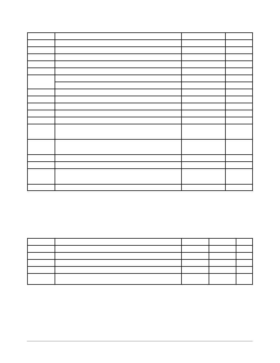
MAXIMUM RATINGS
Symbol
Parameter
Value
Unit
VCC
DC Supply Voltage
0.5 to +7.0
V
VIN
Control Pin Input Voltage
0.5 to +7.0
V
VI/O
Switch Input / Output Voltage
0.5 to +7.0
V
IIK
Control Pin DC Input Diode Current
VIN < GND
50
mA
IOK
Switch I/O Port DC Diode Current
VI/O < GND
50
mA
IO
ONState Switch Current
$128
mA
Continuous Current Through VCC or GND
$150
mA
ICC
DC Supply Current Per Supply Pin
$150
mA
IGND
DC Ground Current per Ground Pin
$150
mA
TSTG
Storage Temperature Range
65 to +150
°C
TL
Lead Temperature, 1 mm from Case for 10 Seconds
260
°C
TJ
Junction Temperature Under Bias
150
°C
qJA
Thermal Resistance
UDFN8 (Note 1)
ULLGA8
Micro8
111
455
392
°C/W
PD
Power Dissipation in Still Air at 85°C
UDFN8
ULLGA8
Micro8
1127
274
319
mW
MSL
Moisture Sensitivity
Level 1
FR
Flammability Rating Oxygen Index: 28 to 34
UL 94 V0 @ 0.125 in
VESD
ESD Withstand Voltage
Human Body Mode (Note 2)
Machine Model (Note 3)
Charged Device Model (Note 4)
> 2000
> 200
N/A
V
ILATCHUP
$200
mA
Stresses exceeding Maximum Ratings may damage the device. Maximum Ratings are stress ratings only. Functional operation above the
Recommended Operating Conditions is not implied. Extended exposure to stresses above the Recommended Operating Conditions may affect
device reliability.
1. Measured with minimum pad spacing on an FR4 board, using 10 mmby1 inch, 2 ounce copper trace no air flow.
2. Tested to EIA / JESD22A114A.
3. Tested to EIA / JESD22A115A.
4. Tested to JESD22C101A.
5. Tested to EIA / JESD78.
RECOMMENDED OPERATING CONDITIONS
Symbol
Parameter
Min
Max
Unit
VCC
Positive DC Supply Voltage
4.0
5.5
V
VIN
Control Pin Input Voltage
0
5.5
V
VI/O
Switch Input / Output Voltage
0
5.5
V
TA
Operating FreeAir Temperature
55
+125
°C
Dt/DV
Input Transition Rise or Fall Rate
Control Input
Switch I/O
0
5
DC
nS/V
相关PDF资料 |
PDF描述 |
|---|---|
| DS1868-50+ | IC POT DIGITAL DUAL 50K 14-DIP |
| 7WB3126BMX1TCG | IC TRANSLATOR 2BIT BUS SW 8LLGA |
| 7WB3126AMX1TCG | IC TRANSLATOR 2BIT BUS SW 8LLGA |
| VI-BW4-MV | CONVERTER MOD DC/DC 48V 150W |
| DS1868-100+ | IC POT DIGITAL DUAL 100K 14-DIP |
相关代理商/技术参数 |
参数描述 |
|---|---|
| 7WB3126DMR2G | 制造商:ONSEMI 制造商全称:ON Semiconductor 功能描述:2-Bit Bus Switch |
| 7WB3126MUTAG | 功能描述:总线发射器 2 BIT TRANSLATING BUS SW RoHS:否 制造商:Texas Instruments 数据速率:135 Mpps 接口: 电源电压-最大:3.6 V 电源电压-最小:3 V 最大工作温度:+ 70 C 安装风格:SMD/SMT 封装 / 箱体:TSSOP-56 封装:Reel |
| 7WB3305 | 制造商:ONSEMI 制造商全称:ON Semiconductor 功能描述:2-Bit Bus Switch |
| 7WB3305AMX1TCG | 功能描述:转换 - 电压电平 2Bit Translating Bus SW 2 Circuit 274mW RoHS:否 制造商:Micrel 类型:CML/LVDS/LVPECL to LVCMOS/LVTTL 传播延迟时间:1.9 ns 电源电流:14 mA 电源电压-最大:3.6 V 电源电压-最小:3 V 最大工作温度:+ 85 C 安装风格:SMD/SMT 封装 / 箱体:MLF-8 |
| 7WB3305BMX1TCG | 功能描述:转换 - 电压电平 2Bit Translating Bus SW 2 Circuit 274mW RoHS:否 制造商:Micrel 类型:CML/LVDS/LVPECL to LVCMOS/LVTTL 传播延迟时间:1.9 ns 电源电流:14 mA 电源电压-最大:3.6 V 电源电压-最小:3 V 最大工作温度:+ 85 C 安装风格:SMD/SMT 封装 / 箱体:MLF-8 |
发布紧急采购,3分钟左右您将得到回复。