- 您现在的位置:买卖IC网 > PDF目录101408 > 8100611EX (MAXIM INTEGRATED PRODUCTS INC) 1-CHANNEL, SGL POLE DOUBLE THROW SWITCH, CDIP16 PDF资料下载
参数资料
| 型号: | 8100611EX |
| 厂商: | MAXIM INTEGRATED PRODUCTS INC |
| 元件分类: | 多路复用及模拟开关 |
| 英文描述: | 1-CHANNEL, SGL POLE DOUBLE THROW SWITCH, CDIP16 |
| 封装: | CERAMIC, DIP-16 |
| 文件页数: | 8/13页 |
| 文件大小: | 347K |
| 代理商: | 8100611EX |
MAX4901–MAX4905
Low-RON, Dual-SPST/Single-SPDT Clickless
Switches with Negative Rail Capability
4
_______________________________________________________________________________________
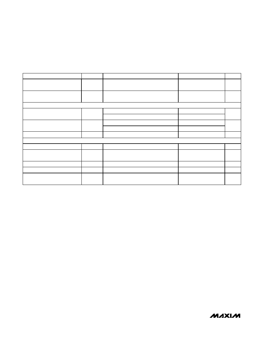
PARAMETER
SYMBOL
CONDITIONS
MIN
TYP
MAX
UNITS
NO_, NC Off-Capacitance
CNO_(OFF)
CNC(OFF)
f = 1MHz, VCOM = 0.5VP-P, DC bias = 0
(Figure 5)
40
pF
COM On-Capacitance
CCOM_(ON)
f = 1MHz, VCOM = 0.5VP-P, DC bias = 0
(Figure 5)
200
pF
DIGITAL I/O (IN_)
VCC = 2.7V to 3.6V
1.4
Input Logic-High Voltage
VIH
VCC = 4.2V to 5.5V
2.0
V
VCC = 2.7V to 3.6V
0.5
Input Logic-Low Voltage
VIL
VCC = 4.2V to 5.5V
0.8
V
Input Leakage Current
IIN
VIN_ = 0V or VCC
-1
+1
A
COMPARATOR (MAX4905)
Comparator Threshold
VCC / 3
V
Comparator Output-High Voltage
ISOURCE = 1mA
VCC -
0.4V
V
Comparator Output-Low Voltage
ISINK = 1mA
0.4
V
Comparator Input Leakage
VCMP- = 0 to 2.7V
-100
+100
nA
Comparator Switching Time
VCC = 2.7V, VCMP- = 0V to VCC, from 50%
of VCMP- to 50% of VCMPO
12
s
Note 1: UCSP and TDFN parts are 100% tested at TA = +25°C only, and guaranteed by design over the specified temperature
range.
Note 2: Signals on COM_, NO_, or NC exceeding VCC are clamped by internal diodes. Limit forward-diode current to maximum cur-
rent rating.
Note 3: Guaranteed by design.
Note 4: ICOM for UCSP is 10mA.
Note 5:
RON = RON(MAX) – RON(MIN).
Note 6: Flatness is defined as the difference between the maximum and minimum value of on-resistance as measured over the
specified analog signal ranges.
Note 7: The MAX4902/MAX4904/MAX4905 have an internal shunt resistor when, in off-state, will determine off-current.
Note 8: Off-Isolation = 20log10 (VCOM / VNO), VCOM = output, VNO = input to off switch.
ELECTRICAL CHARACTERISTICS (continued)
(VCC = +2.7V to +5.5V, TA = -40°C to +85°C, unless otherwise noted. Typical values are at VCC = +3.0V, TA = +25°C, unless other-
wise noted.) (Note 1)
相关PDF资料 |
PDF描述 |
|---|---|
| 89579-934LF | TWO PART BOARD CONNECTOR |
| 89579-936LF | TWO PART BOARD CONNECTOR |
| 89696-004LF | TWO PART BOARD CONNECTOR |
| 89696-006LF | TWO PART BOARD CONNECTOR |
| 89696-008LF | TWO PART BOARD CONNECTOR |
相关代理商/技术参数 |
参数描述 |
|---|---|
| 81006122A | 制造商:Intersil Corporation 功能描述:ANLG SW DUAL SPDT NRV - Rail/Tube |
| 81006122X | 制造商:未知厂家 制造商全称:未知厂家 功能描述:SPDT Analog Switch |
| 8100612EA | 功能描述:模拟开关 IC CMOS TTL Compatible RoHS:否 制造商:Texas Instruments 开关数量:2 开关配置:SPDT 开启电阻(最大值):0.1 Ohms 切换电压(最大): 开启时间(最大值): 关闭时间(最大值): 工作电源电压:2.7 V to 4.5 V 最大工作温度:+ 85 C 安装风格:SMD/SMT 封装 / 箱体:DSBGA-16 |
| 8100612EA/MLB | 制造商:Harris Corporation 功能描述: |
| 8100612EX | 制造商:未知厂家 制造商全称:未知厂家 功能描述:SPDT Analog Switch |
发布紧急采购,3分钟左右您将得到回复。