- 您现在的位置:买卖IC网 > PDF目录357530 > 8P008SRV3104I15 (WHITE ELECTRONIC DESIGNS CORP) 4M X 16 MULTI DEVICE SRAM CARD, 150 ns, XMA68 PDF资料下载
参数资料
| 型号: | 8P008SRV3104I15 |
| 厂商: | WHITE ELECTRONIC DESIGNS CORP |
| 元件分类: | SRAM |
| 英文描述: | 4M X 16 MULTI DEVICE SRAM CARD, 150 ns, XMA68 |
| 封装: | CARD2-68 |
| 文件页数: | 4/10页 |
| 文件大小: | 120K |
| 代理商: | 8P008SRV3104I15 |
January 2002 Rev. 0 - ECO #xxxx
4
PCMCIA SRAM Memory Card
SRV30 Series
PC Card Products
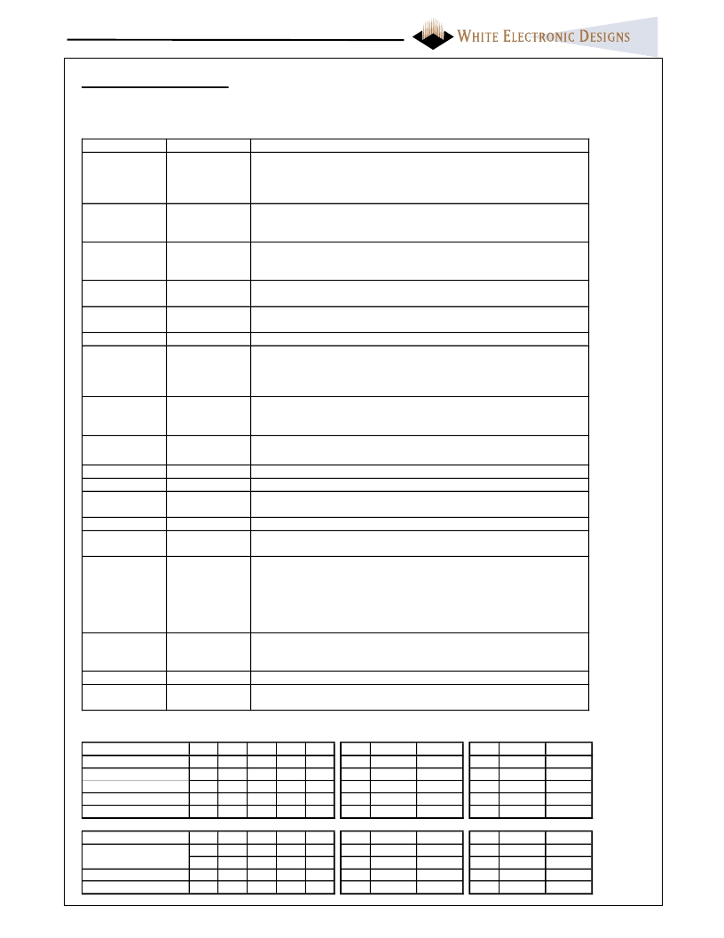
Symbol
A0 - A25
Type
Name and Function
INPUT
ADDRESS INPUTS:
A0 through A25 enable direct addressing of up
to 64MB of memory on the card. Signal A0 is not used in word access
mode. A25 is the most significant bit. (address pins used are based on
card density,see pinout for highest used address pin)
DATA INPUT/OUTPUT:
DQ0 THROUGH DQ15 constitute the
bi-directional databus. DQ0 - DQ7 constitute the lower (even) byte and
DQ8 - DQ15 the upper (odd) byte. DQ15 is the MSB.
CARD ENABLE 1 AND 2:
CE1# enables even byte accesses, CE2#
enables odd byte accesses. Multiplexing A0, CE1# and CE2# allows 8-
bit hosts to access all data on DQ0 - DQ7.
OUTPUT ENABLE:
Active low signal enabling read data from the
memory card.
WRITE ENABLE:
Active low signal gating write data to the memory
card.
READY /BUSY OUTPUT:
Not used for SRAM cards
CARD DETECT 1 and 2:
Provide card insertion detection. T hese
signals are connected to ground internally on the memory card. The
host socket interface circuitry shall supply 10K-ohm or larger pull-up
resistors on these signal pins.
WRITE PROTECT:
Follows hardware Write Protect Switch. When
Switch is placed in on position, signal is pulled high (10K ohm). When
switch is off signal is pulled low.
PROGRAM/ERASE POWER SUPPLY:
Not used for SRAM
cards.
CARD POWER SUPPLY :
3.3V / 5.0V for all internal circuitry.
GROUND:
for all internal circuitry.
ATTRIBUTE MEMORY SELECT :
only used with cards built with
optional attribute memory.
RESET:
Not used for SRAM cards
WAIT:
This signal is pulled high internally for compatibility. No wait
states are generated.
BATTERY V OLTAGE DETECT:
Provides status of Battery
voltage.
BVD2 = BVD1 = Voh (battery voltage is guaranteed to retain data)
BVD2 = Vol, BVD1 = Voh (data is valid, battery recharge required)
BVD2 = BVD1 = Vol (data may no longer be valid, battery requires
extended recharge)
VOLTAGE SENSE:
Notifies the host socket of the card's VCC
requirements. VS1 is grounded and VS2 is open to indicate a 3.3V/5V
16 bit card, with a 5V key, has been inserted.
RESERVED FOR FUTURE USE
NO INTERNAL CONNECTION TO CARD:
pin may be driven
or left floating
DQ0 - DQ15
INPUT/OUT
PUT
CE1#, CE2#
INPUT
OE#
INPUT
WE#
INPUT
RDY /BSY #
CD1#, CD2#
OUT PUT
OUT PUT
WP
OUT PUT
VPP1, VPP2
N.C.
VCC
GND
REG#
INPUT
RST
WAIT #
INPUT
OUT PUT
BVD1, BVD2
OUT PUT
VS1, VS2
OUT PUT
RFU
N.C.
Card Signal Description
FUNCTIONAL TRUTH TABLE
READ function
Function Mode
Standby Mode
Byte Access (8 bits)
Common Memory
/REG
D15-D8
X
High-Z
H
High-Z
H
High-Z
H
Odd-Byte Even-Byte
H
Odd-Byte
Attribute Memory
/REG
D15-D8
X
High-Z
L
High-Z
L
High-Z
L
Not Valid Even-Byte
L
Not Valid
/CE2 /CE1
H
H
H
L
L
A0
X
L
H
X
X
/OE
X
L
L
L
L
/WE
X
H
H
H
H
D7-D0
High-Z
Even-Byte
Odd-Byte
D7-D0
High-Z
Even-Byte
Not Valid
H
L
L
L
H
Word Access (16 bits)
Odd-Byte Only Access
WRITE function
Standby Mode
Byte Access (8 bits)
High-Z
High-Z
H
H
H
L
L
H
L
L
L
H
X
L
H
X
X
X
H
H
H
H
X
L
L
L
L
X
H
H
H
H
X
X
X
X
X
L
L
L
L
X
X
X
X
X
X
Even-Byte
Odd-Byte
Even-Byte
X
Even-Byte
X
Word Access (16 bits)
Odd-Byte Only Access
Odd-Byte Even-Byte
Odd-Byte
X
相关PDF资料 |
PDF描述 |
|---|---|
| 8P016SRV3101I15 | 8M X 16 MULTI DEVICE SRAM CARD, 150 ns, XMA68 |
| 8P008SRV3205I15 | 4M X 16 MULTI DEVICE SRAM CARD, 150 ns, XMA68 |
| 8P016SRV3104C15 | 8M X 16 MULTI DEVICE SRAM CARD, 150 ns, XMA68 |
| 8P016SRV3300C15 | 8M X 16 MULTI DEVICE SRAM CARD, 150 ns, XMA68 |
| 8P016SRV3301I15 | 8M X 16 MULTI DEVICE SRAM CARD, 150 ns, XMA68 |
相关代理商/技术参数 |
参数描述 |
|---|---|
| 8P-03AFFM-QL5A01 | 功能描述:M8 CONN 制造商:amphenol ltw 系列:* 零件状态:在售 标准包装:10 |
| 8P-03AFFM-QL5A02 | 功能描述:M8 CONN 制造商:amphenol ltw 系列:* 零件状态:在售 标准包装:10 |
| 8P-03AFFM-QL5A05 | 功能描述:M8 CONN 制造商:amphenol ltw 系列:* 零件状态:在售 标准包装:10 |
| 8P-03AFFM-QL5A10 | 功能描述:M8 CONN 制造商:amphenol ltw 系列:* 零件状态:在售 标准包装:10 |
| 8P-03AFFM-QL5B01 | 功能描述:M8 CONN 制造商:amphenol ltw 系列:* 零件状态:在售 标准包装:10 |
发布紧急采购,3分钟左右您将得到回复。