- 您现在的位置:买卖IC网 > PDF目录24623 > 9248YF-20LF (INTEGRATED DEVICE TECHNOLOGY INC) PROC SPECIFIC CLOCK GENERATOR, PDSO48 PDF资料下载
参数资料
| 型号: | 9248YF-20LF |
| 厂商: | INTEGRATED DEVICE TECHNOLOGY INC |
| 元件分类: | 时钟产生/分配 |
| 英文描述: | PROC SPECIFIC CLOCK GENERATOR, PDSO48 |
| 封装: | 0.300 INCH, ROHS COMPLIANT, MO-118, SSOP-48 |
| 文件页数: | 1/12页 |
| 文件大小: | 181K |
| 代理商: | 9248YF-20LF |
Integrated
Circuit
Systems, Inc.
General Description
Features
ICS9248-20
0276E—12/15/08
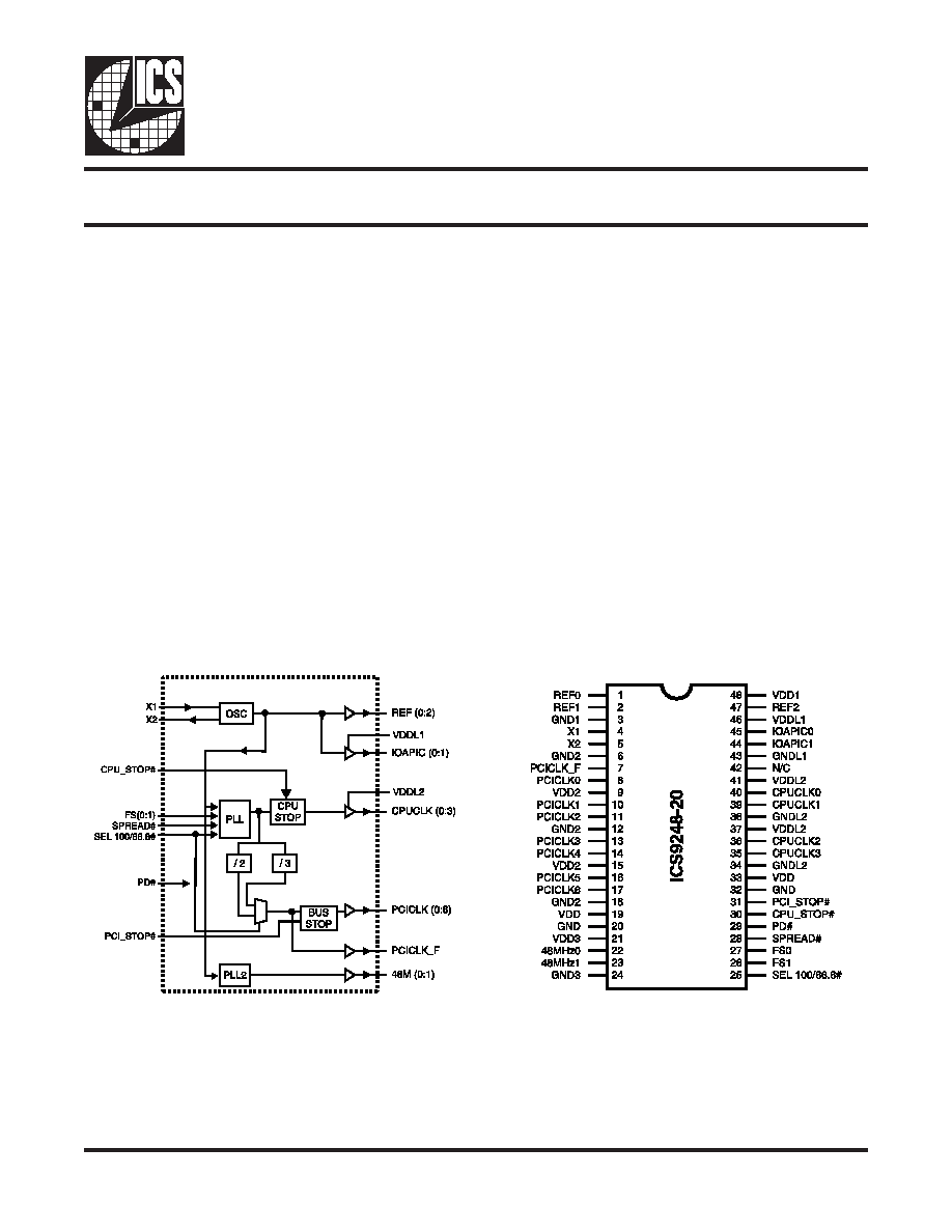
Block Diagram
Pentium/ProTM System Clock Chip
Pin Configuration
48-Pin SSOP
Generates system clocks for CPU, IOAPIC, PCI,
plus 14.314 MHz REF (0:2), USB, and Super I/O
Supports single or dual processor systems
Supports Spread Spectrum modulation for CPU &
PCI clocks, down spread -0.5%
Skew from CPU (earlier) to PCI clock (rising edges
for 100/33.3MHz) 1.5 to 4ns
Two fixed outputs at 48MHz.
Separate 2.5V and 3.3V supply pins
2.5V or 3.3V output: CPU, IOAPIC
3.3V outputs: PCI, REF, 48MHz
No power supply sequence requirements
Uses external 14.318MHz crystal, no external load
cap required for CL=18pF crystal
48 pin 300 mil SSOP
The ICS9248-20 is a Clock Synthesizer chip for Pentium
and PentiumPro CPU based Desktop/Notebook systems
that will provide all necessary clock timing.
Features include four CPU and eight PCI clocks. Three
reference outputs are available equal to the crystal
frequency. Additionally, the device meets the Pentium
power-up stabilization requirement, assuring that CPU
and PCI clocks are stable within 2ms after power-up.
PD# pin enables low power mode by stopping crystal OSC
and PLL stages. Other power management features
include CPU_STOP#, which stops CPU (0:3) clocks, and
PCI_STOP#, which stops PCICLK (0:6) clocks.
High drive CPUCLK outputs typically provide greater than
1 V/ns slew rate into 20pF loads. PCICLK outputs typically
provide better than 1V/ns slew rate into 30pF loads while
maintaining 50±5% duty cycle. The REF clock outputs
typically provide better than 0.5V/ns slew rates.
The ICS9248-20 accepts a 14.318MHz reference crystal
or clock as its input and runs on a 3.3V core supply.
Power Groups
VDD = Supply for PLL core
VDD1 = REF (0:2), X1, X2
VDD2 = PCICLK_F, PCICLK (0:6)
VDD3 = 48MHz0, 48MHz1
VDDL1 = IOAPIC (0:1)
VDDL2 = CPUCLK (0:3)
Ground Groups
GND = Ground for PLL core
GND1 = REF (0:2), X1, X2
GND2 = PCICLK_F, PCICLK (0:6)
GND3 = 48MHz0, 48MHz1
GNDL1 = IOAPIC (0:1)
GNDL2 = CPUCLK (0:3)
相关PDF资料 |
PDF描述 |
|---|---|
| 9248YF-65 | PROC SPECIFIC CLOCK GENERATOR, PDSO48 |
| 9248YF-95LF | 124 MHz, PROC SPECIFIC CLOCK GENERATOR, PDSO48 |
| 051-928-9019 | RF Coaxial Connectors |
| 9248YG-92GLFT | PROC SPECIFIC CLOCK GENERATOR, PDSO48 |
| 924AB4XM-L2P | PROXIMITY SENSOR-INDUCTIVE, 4.5-9.5mm, 1-9V, CYLINDRICAL |
相关代理商/技术参数 |
参数描述 |
|---|---|
| 9248YF-50-T | 制造商:ICS 制造商全称:ICS 功能描述:Frequency Timing Generator for Pentium II Systems |
| 9249 | 制造商:Apex Tool Group 功能描述:PUSH ROD FOR 9290 SERIES PNEUMATIC CUTTER |
| 924922-000 | 制造商:TE Connectivity 功能描述:Heat Shrink Flexible Molded Boot ST Polyolefin 制造商:TE Connectivity 功能描述:BOOT FLXBL MOD POLYFN - Bulk 制造商:TE Connectivity 功能描述:BOOT MOLDED |
| 924924-000 | 制造商:TE Connectivity 功能描述:114-WP110X |
| 92495160 | 制造商:Glenair Inc 功能描述:MICRO-D CONNECTORS - Bulk |
发布紧急采购,3分钟左右您将得到回复。