- 您现在的位置:买卖IC网 > PDF目录24767 > 935024370602 (NXP SEMICONDUCTORS) TRIPLE LINE TRANSCEIVER, PDIP16 PDF资料下载
参数资料
| 型号: | 935024370602 |
| 厂商: | NXP SEMICONDUCTORS |
| 元件分类: | Buffer和线驱动 |
| 英文描述: | TRIPLE LINE TRANSCEIVER, PDIP16 |
| 封装: | PLASTIC, DIP-16 |
| 文件页数: | 2/5页 |
| 文件大小: | 50K |
| 代理商: | 935024370602 |
Philips Semiconductors Linear Products
Product specification
MC145406
EIA-232-D/V.28 driver/receiver
August 31, 1994
468
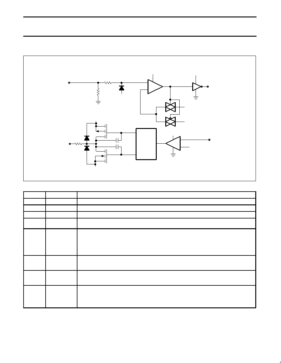
BLOCK DIAGRAM
RECEIVER
DO
DI
1.4V
LEVEL
SHIFT
DRIVER
HYSTERESIS
300
15k
5.4k
RX
TX
VCC
VSS
VCC
VDD
VSS
VCC
1.0V
1.8V
+
–
+
–
PIN #
SYMBOL
PIN DESCRIPTION
1
VDD
Positive power supply. The most positive power supply pin, which is typically 5 to 12 volts.
8
VSS
Negative power supply. The most negative power supply pin, which is typically -5 to -12 volts.
16
VCC
Digital power supply. The digital supply pin, which is connected to the logic power supply (maximum +5.5V).
9
GND
Ground. Ground return pin is typically connected to the signal ground pin of the EIA-232-D connector (Pin 7)
as well as to the logic power supply ground.
2, 4, 6
RX1, RX2, RX3
Receive Data Input. These are the EIA-232-D receive signal inputs whose voltages can range from +25 to
-25V. A voltage between +3 and +25 is decoded as a space and causes the corresponding DO pin to swing
to ground (0V); a voltage between -3 and -25V is decoded as a mark and causes the DO pin to swing up to VCC.
The actual turn-on input switchpoint is typically biased at 1.8V above ground, and includes 800mV of hysteresis
for noise rejection. The nominal input impedance is 5k
. An open or grounded input pin is interpreted as a mark,
forcing the DO pin to VCC.
11, 13, 15
DO1, DO2, DO3
Data Output. These are the receiver digital output pins, which swing from VCC to GND. A space on the RX
pin causes DO to produce a logic zero; a mark produces a logic one. Each output pin is capable of driving one
LSTTL input load.
10, 12, 14
DI1, DI2, DI3
Data Input. These are the high-impedance digital input pins to the drivers. TTL compatibility is accomplished
by biasing the input switchpoint at 1.4V above ground. However, 5V CMOS compatibility is maintained as well.
Input voltage levels on these pins must be between VCC and GND.
3, 5, 7
TX1, TX2, TX3
Transmit Data Output. These are the EIA-232-D transmit signal output pins, which swing toward VDD and VSS.
A logic one at a DI input causes the corresponding TX output to swing toward VSS. A logic zero causes the
output to swing toward VDD (the output voltages will be slightly less than VDD or VSS depending upon the output
load). Output slew rates are limited to a maximum of 30V/
s. When the MC145406 is off (VDD = VSS = VCC
= GND), the minimum output impedance is 300
.
相关PDF资料 |
PDF描述 |
|---|---|
| 935024380129 | TRIPLE LINE TRANSCEIVER, PDSO16 |
| 0640-1215T | Analog IC |
| 935024380602 | TRIPLE LINE TRANSCEIVER, PDSO16 |
| 0640-1216T | Analog IC |
| 935024380623 | TRIPLE LINE TRANSCEIVER, PDSO16 |
相关代理商/技术参数 |
参数描述 |
|---|---|
| 9-350255-1 | 制造商:TE CONNECTIVITY 功能描述:CONNECTOR |
| 9-350264-1 | 制造商:TE CONNECTIVITY 功能描述:CONNECTOR 制造商:TE Connectivity / AMP 功能描述: |
| 935027-000 | 制造商:TE Connectivity 功能描述:High Performance Cable 制造商:TE Connectivity 功能描述:55A1811-8-9-9CS2275 - Cable Rools/Shrink Tubing |
| 9350-2R1 | 制造商:Johanson Manufacturing 功能描述:VARIABLE CAPACITOR 制造商:Johanson 功能描述:9350-2R1 |
| 9350301 | 功能描述:工业压力 / 力传感器 SST PRESS TRANSDUCER RoHS:否 制造商:Honeywell 工作压力:0 bar to 25 bar 压力类型:Sealed Gauge 准确性:0.25 % 输出类型: 安装风格:Screw 工作电源电压:8 V to 30 V 输出电压:8 V to 30 V 封装: |
发布紧急采购,3分钟左右您将得到回复。