- 您现在的位置:买卖IC网 > PDF目录122717 > 935056380512 (NXP SEMICONDUCTORS) 8 CHANNEL(S), 115.2K bps, SERIAL COMM CONTROLLER, PQCC84 PDF资料下载
参数资料
| 型号: | 935056380512 |
| 厂商: | NXP SEMICONDUCTORS |
| 元件分类: | 微控制器/微处理器 |
| 英文描述: | 8 CHANNEL(S), 115.2K bps, SERIAL COMM CONTROLLER, PQCC84 |
| 封装: | PEDESTAL, PLASTIC, MO-047AF, SOT-189-3, LCC-84 |
| 文件页数: | 11/29页 |
| 文件大小: | 167K |
| 代理商: | 935056380512 |
第1页第2页第3页第4页第5页第6页第7页第8页第9页第10页当前第11页第12页第13页第14页第15页第16页第17页第18页第19页第20页第21页第22页第23页第24页第25页第26页第27页第28页第29页
Philips Semiconductors
Product specification
SCC2698B
Enhanced octal universal asynchronous
receiver/transmitter (Octal UART)
2000 Jan 31
19
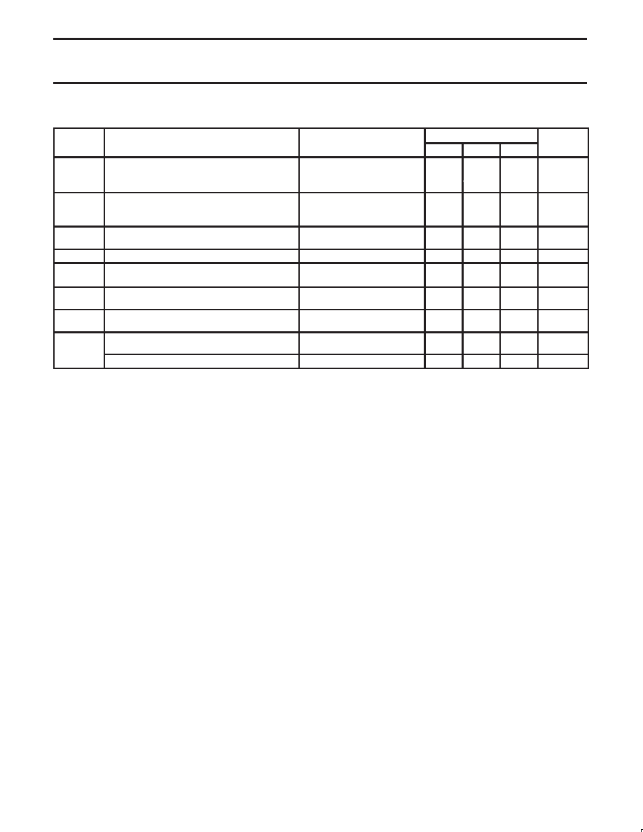
DC ELECTRICAL CHARACTERISTICS1, 2, 3 TA = 0 to +70_, VCC = 5.0 V " 10%, –40 to 85_C
SYMBOL
PARAMETER
TEST CONDITIONS
LIMITS
UNIT
SYMBOL
PARAMETER
TEST CONDITIONS
Min
Typ
Max
UNIT
VIL
Input low voltage
0.8
V
VIH
Input high voltage (except X1/CLK)
2.0
V
VIH
Input high voltage (X1/CLK)
0.8VCC
V
VOL
VOH
Output Low voltage
Output High voltage (except OD outputs)
IOL = 2.4mA
IOH = –400A
IOH = –100A
0.8VCC
0.9VCC
0.4
V
IIL
IIH
Input current Low, MPI and MPP pins
Input current High, MPI and MPP pins
VIN = 0
VIN = VCC
–50
20
A
II
Input leakage current
VIN = 0 to VCC
–10
10
A
IILX1
IIHX1
X1/CLK input Low current
X1/CLK input High current
VIN = GND, X2 = open
VIN = VCC, X2 = open
–100
100
A
IOZH
IOZL
Output off current High, 3-State data bus
Output off current Low, 3-State data bus
VIN = VCC
VIN = 0
–10
10
A
IODL
IODH
Open-drain output Low current in off state: IRQN
VIN = VCC
VIN = 0
–10
10
A
ICC
Power supply current
Operating mode
30
mA
ICC
Power down mode9
2.0
mA
NOTES:
1. Parameters are valid over specified temperature range. See ordering information table for applicable temperature range and operating
supply range.
2. All voltage measurements are referenced to ground (GND). For testing, all inputs swing between 0.4V and 2.4V with a transition time of 20ns
maximum. For X1/CLK this swing is between 0.4V and 4.4V. All time measurements are referenced at input voltages of VIL and VIH, as
appropriate.
3. Typical values are at +25
°C, typical supply voltages, and typical processing parameters.
4. Test condition for interrupt and MPP outputs: CL = 50pF, RL = 2.7k to VCC. Test conditions for rest of outputs: CL = 150pF.
5. Timing is illustrated and referenced to the WRN and RDN inputs. The device may also be operated with CEN as the ‘strobing’ input. CEN
and RDN (also CEN and WRN) are ANDed internally. As a consequence, the signal asserted last initiates the cycle and the signal negated
first terminates the cycle.
6. If CEN is used as the ‘strobing’ input, the parameter defines the minimum high times between one CEN and the next. The RDN signal must
be negated for tRWD guarantee that any status register changes are valid.
7. Consecutive write operations to the command register require at least three edges of the X1 clock between writes.
8. This value is not tested, but is guaranteed by design.
9. See UART applications note for power down currents less than 5
A.
10. Operation to 0MHz is assured by design. Minimum test frequency is 2MHz.
11. Address is latched on leading edge of read or write cycle.
相关PDF资料 |
PDF描述 |
|---|---|
| 932S203YGT | 133.3 MHz, PROC SPECIFIC CLOCK GENERATOR, PDSO56 |
| 935069310118 | I2C BUS CONTROLLER, PDSO20 |
| 9LRS3187BKLF | 133.33 MHz, PROC SPECIFIC CLOCK GENERATOR, PQCC32 |
| 935262233118 | 16 I/O, PIA-GENERAL PURPOSE, PDSO24 |
| 935262403118 | 0 TIMER(S), REAL TIME CLOCK, PDSO8 |
相关代理商/技术参数 |
参数描述 |
|---|---|
| 9350569 | 制造商:WIKA INSTRUMENTS 功能描述:1/8,1/4 GAUGE |
| 93505A180 | 制造商:MISC. SPCR/STNDF/HND 功能描述: |
| 93505A43 | 制造商:FLORIDA MISC. 功能描述: 制造商:Florida Misc. 功能描述: |
| 93505A435 | 制造商:FLORIDA MISC. 功能描述: 制造商:Florida Misc. 功能描述: |
| 93505A810 | 制造商:FLORIDA MISC. 功能描述: |
发布紧急采购,3分钟左右您将得到回复。