- 您现在的位置:买卖IC网 > PDF目录24830 > 935269077118 (NXP SEMICONDUCTORS) CBT/FST/QS/5C/B SERIES, 10 1-BIT DRIVER, TRUE OUTPUT, PDSO24 PDF资料下载
参数资料
| 型号: | 935269077118 |
| 厂商: | NXP SEMICONDUCTORS |
| 元件分类: | 总线收发器 |
| 英文描述: | CBT/FST/QS/5C/B SERIES, 10 1-BIT DRIVER, TRUE OUTPUT, PDSO24 |
| 封装: | 4.40 MM, PLASTIC, MO-153, SOT-355-1, TSSOP-24 |
| 文件页数: | 6/10页 |
| 文件大小: | 112K |
| 代理商: | 935269077118 |
Philips Semiconductors
Product data
CBTS3384
10-bit bus switch with 5-bit output enables
and Schottky undershoot protection
2002 Dec 13
4
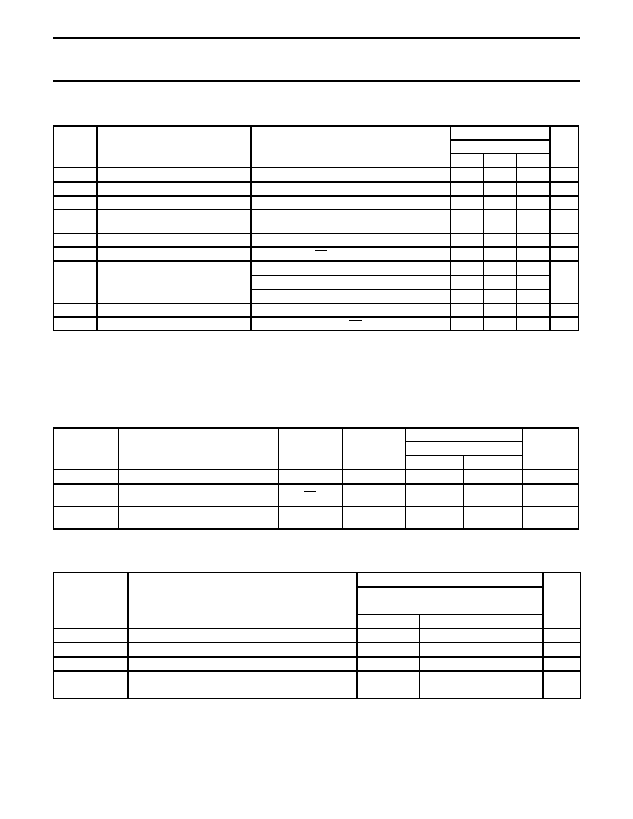
DC ELECTRICAL CHARACTERISTICS
LIMITS
SYMBOL
PARAMETER
TEST CONDITIONS
Tamb = -40 to +85 °C
UNIT
Min
Typ1
Max
VIK
Input clamp voltage
VCC = 4.5 V; II = -18 mA
—
-1.2
V
II
Input leakage current
VCC = 5.5 V; VI = GND or 5.5 V
—
±1
A
ICC
Quiescent supply current2
VCC = 5.5 V; IO = 0, VI = VCC or GND
—
3
A
ICC
Additional supply current per input pin2
VCC = 5.5 V, one input at 3.4 V, other inputs at VCC
or GND
—
2.5
mA
CI
Control pins
VI= 3.0 V or 0
—
4
—
pF
CI(OFF)
Power-off leakage current
VO = 3.0 V or 0, OE = VCC
—
10
—
pF
VCC = 4.5 V; VI = 0 V; II = 64 mA
—
5
7
ron3
On-resistance
VCC = 4.5 V; VI = 0 V; II = 30 mA
—
5
7
on
VCC = 4.5 V; VI = 2.4 V; II = -15 mA
—
10
15
VP
Pass voltage
VI= VCC = 5.0 V; IO = -100 A
3.4
3.6
3.9
V
IUCP
Undershoot static current protection
VCC = 5.0 V, IB = 400 A; OE = 5.0 V; VB ≥ 3.0 V
—
8
—
mA
NOTES:
1. All typical values are at VCC = 5 V, Tamb = 25 °C.
2. This is the increase in supply current for each input that is at the specified TTL voltage level rather than VCC or GND.
3. Measured by the voltage drop between the A and the B terminals at the indicated current through the switch. On-state resistance is
determined by the lowest voltage of the two (A or B) terminals.
AC CHARACTERISTICS
GND = 0 V; tR; CL = 50 pF
LIMITS
SYMBOL
PARAMETER
FROM
TO
VCC = +5.0 V ±0.5 V
UNIT
(INPUT)
(OUTPUT)
Min
Max
tpd
Propagation delay1
A or B
B or A
—
0.25
ns
ten
Output enable time
to High and Low level
OE
A or B
1.0
5.7
ns
tdis
Output disable time
from High and Low level
OE
A or B
1.0
5.2
ns
NOTE:
1. This parameter is warranted but not production tested. The propagation delay is based on the RC time constant of the typical on-state
resistance of the switch and a load capacitance of 50 pF, when driven by an ideal voltage source (zero output impedance).
LIMITS
SYMBOL
PARAMETER DESCRIPTION
-40 to +85
° C
VCC = 5 V, ±0.5 V
UNIT
MIN.
MEAN
MAX.
tPD
Propagation delay (see Note 1)
—
250
pS
tPZH
Output enable time to High level
1.6
3.4
5.6
nS
tPHZ
Output enable time from High level
1.7
3.3
5.5
nS
tPZL
Output enable time to Low level
2.3
4
6
nS
tPLZ
Output enable time from Low level
2.5
4.5
6.6
nS
NOTE:
1. This parameter is warranted but not production tested. The propagation delay is based on the RC time constant of the typical on-state
resistance of the switch and a load capacitance of 50 pF, when driven by an ideal voltage source (zero output impedance); at +25
°C.
相关PDF资料 |
PDF描述 |
|---|---|
| 0803-6204-01 | ISDN U Interface Hybrid |
| 935269117118 | LINE TRANSCEIVER, PBCC16 |
| 935269117115 | LINE TRANSCEIVER, PBCC16 |
| 935267286118 | LINE TRANSCEIVER, PDSO16 |
| 935267286112 | LINE TRANSCEIVER, PDSO16 |
相关代理商/技术参数 |
参数描述 |
|---|---|
| 935269304128 | 制造商:ST-Ericsson 功能描述:IC AUDIO CODEC W/TCH SCRN 48LQFP |
| 935269544557 | 制造商:NXP Semiconductors 功能描述:SUB ONLY TDA9587-2US1-V1.3 |
| 935269987557 | 制造商:NXP Semiconductors 功能描述:SUB ONLY TDA9587-1US1-V1.8 SUBBED TO 935269987557 |
| 935270713557 | 制造商:NXP Semiconductors 功能描述:SUB ONLY IC CHP |
| 935270792551 | 制造商:NXP Semiconductors 功能描述:IC BUFF DVR TRI-ST 16BIT 56VFBGA |
发布紧急采购,3分钟左右您将得到回复。