- 您现在的位置:买卖IC网 > PDF目录24830 > 935269451118 (NXP SEMICONDUCTORS) 133 MHz, PROC SPECIFIC CLOCK GENERATOR, PDSO56 PDF资料下载
参数资料
| 型号: | 935269451118 |
| 厂商: | NXP SEMICONDUCTORS |
| 元件分类: | 时钟产生/分配 |
| 英文描述: | 133 MHz, PROC SPECIFIC CLOCK GENERATOR, PDSO56 |
| 封装: | 7.50 MM, PLASTIC, MO-118, SOT-371-1, SSOP-56 |
| 文件页数: | 10/16页 |
| 文件大小: | 105K |
| 代理商: | 935269451118 |
Philips Semiconductors
Product specification
PCK2014A
CK98 (100/133 MHz) spread spectrum
system clock generator
2001 Apr 02
3
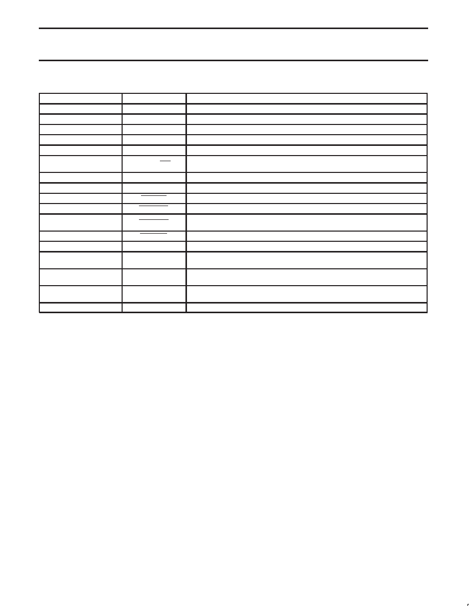
PIN DESCRIPTION
PIN NUMBER
SYMBOL
FUNCTION
2, 3
REF [0–1]
3.3 V 14.318 MHz clock output
5
XTAL_IN
14.318 MHz crystal input
6
XTAL_OUT
14.318 MHz crystal output
9, 11, 12, 14, 15, 18
PCI_[F, 1–5]
3.3 V PCI clock outputs, pin 9 is a free running PCI clock
25, 26
3V66 [0–1]
3.3 V fixed 66 MHz clock outputs
28
SEL133/100
Select input pin for enabling 133 MHz or 100 MHz CPU outputs.
H = 133 MHz, L = 100 MHz
30
48 MHz USB
3.3 V fixed 48 MHZ clock output
32, 33
SEL [0–1]
Logic select pins. TTL levels.
34
SPREAD
3.3 V LVTTL input. Enables spread spectrum mode when held LOW.
35
PWRDWN
3.3 V LVTTL input. Device enters powerdown mode when held LOW.
36
CPUSTOP
3.3 V LVTTL input. Stops all CPU clocks and 3V66 clocks when held LOW.
CPUDIV_2 output remains on all the time.
37
PCISTOP
3.3 V LVTTL input. Stops all PCI clocks except PCICLK_F when held LOW.
41, 42, 45, 46, 49, 50
CPUCLK [0–5]
2.5 V CPU output. 133 MHz or 100 MHz depending on state of input pin SEL133/100.
53, 54, 55
APIC [0–2]
2.5 V clock outputs running divide synchronous with the CPU clock frequency.
Fixed 16.67 MHz limit.
4, 10, 16, 17,
22, 23, 27, 31, 39
VDD3V
3.3 V power supply, pins 22 and 23 are analog VDD.
1, 7, 8, 13, 19, 20, 21, 24,
29, 38, 40, 44, 48, 52
VSS
Ground, pins 20 and 21 are analog VSS.
43, 47, 51, 56
VDD25V
2.5 V power supply
NOTE:
1. VDD3V, VDD25V and VSS in the above table reflects a likely internal POWER and GROUND partition to reduce the effects of internal noise on
the performance of the device. In reality, the platform will be configured with the VDD25V pins tied to a 2.5 V supply, all remaining VDD pins
tied to a common 3.3 V supply and all VSS pins being common.
2. Pins 20 and 21 are analog ground and should be tied to a ground plane. Pins 22 and 23 are analog VDD should be properly decoupled
to a 3.3 V supply. These analog power supply pins should not be tied to the PCI power and ground to avoid noise coupling into the
analog power supply pins. The PCK2014 provides separate power supplies for the internal digital circuitry (pin 39, VCC) and the internal
PLLs of the device (pins 22 and 23, VCC). The purpose of this approach is to try and isolate the high switching noise digital outputs from
relatively sensitive analog blocks. In controlled environments such as a test board this level is very well controlled. However, in a mixed
signal environment, a second level of isolation may be required.
相关PDF资料 |
PDF描述 |
|---|---|
| 935269451112 | 133 MHz, PROC SPECIFIC CLOCK GENERATOR, PDSO56 |
| 0803-7700-03 | VDSL / PSTN CO Splitter |
| 935269471115 | 2.8 V FIXED POSITIVE LDO REGULATOR, 0.06 V DROPOUT, PDSO5 |
| 935269472115 | 3 V FIXED POSITIVE LDO REGULATOR, 0.06 V DROPOUT, PDSO5 |
| 935269473115 | 3.2 V FIXED POSITIVE LDO REGULATOR, 0.055 V DROPOUT, PDSO5 |
相关代理商/技术参数 |
参数描述 |
|---|---|
| 935269544557 | 制造商:NXP Semiconductors 功能描述:SUB ONLY TDA9587-2US1-V1.3 |
| 935269987557 | 制造商:NXP Semiconductors 功能描述:SUB ONLY TDA9587-1US1-V1.8 SUBBED TO 935269987557 |
| 935270713557 | 制造商:NXP Semiconductors 功能描述:SUB ONLY IC CHP |
| 935270792551 | 制造商:NXP Semiconductors 功能描述:IC BUFF DVR TRI-ST 16BIT 56VFBGA |
| 935270792557 | 制造商:NXP Semiconductors 功能描述:IC BUFF DVR TRI-ST 16BIT 56VFBGA |
发布紧急采购,3分钟左右您将得到回复。