- 您现在的位置:买卖IC网 > PDF目录24830 > 935269650115 (NXP SEMICONDUCTORS) 2.8 V FIXED POSITIVE LDO REGULATOR, 0.12 V DROPOUT, PDSO5 PDF资料下载
参数资料
| 型号: | 935269650115 |
| 厂商: | NXP SEMICONDUCTORS |
| 元件分类: | 固定正电压单路输出LDO稳压器 |
| 英文描述: | 2.8 V FIXED POSITIVE LDO REGULATOR, 0.12 V DROPOUT, PDSO5 |
| 封装: | 1.60 MM, PLASTIC, SOT-680-1, SO-5 |
| 文件页数: | 11/16页 |
| 文件大小: | 235K |
| 代理商: | 935269650115 |
Philips Semiconductors
Product data
SA57000-XX
CapFREE
150 mA, low-noise, low dropout regulator
with thermal protection
2003 Apr 01
4
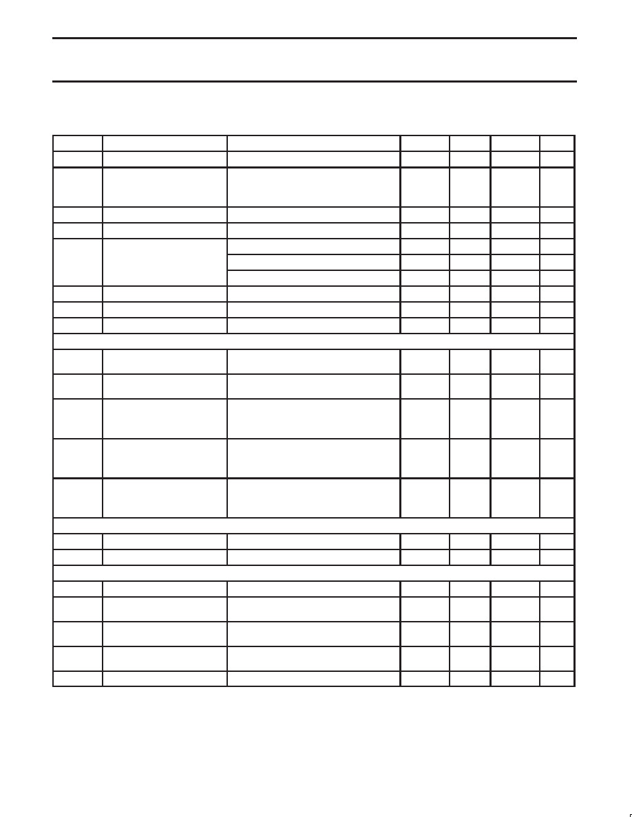
CHARACTERISTICS
VIN = VOUT(nom) + 0.5 V. (Note 1.)
SYMBOL
PARAMETER
CONDITIONS
MIN.
TYP.
MAX.
UNIT
VIN
input voltage
VOUT(nom)
–
6.5
V
output voltage accuracy 2
IOUT = 1 mA
Tamb = +25 °C
–
±1
–
%
–40
°C ≤ Tamb ≤ +85 °C
–2.0
–
2.0
%
ILIM
current limit
160
300
–
mA
IQ
ground pin current
IOUT = 1 mA to 150 mA
–
85
150
A
dropout voltage 3
IOUT = 1 mA
–
1
–
mV
IOUT = 50 mA
–
55
120
mV
IOUT = 150 mA
–
165
–
mV
VLNR
line regulation
VIN = (VOUT + 0.1 V) to 5.5 V; IOUT = 20 mA
–
0.1
%/V
VLDR
load regulation
IOUT = 1 mA to 150 mA
–
0.01
0.02
%/mA
en
output voltage noise
f = 10 Hz to 100 kHz, COUT = 10 F
–
30
–
VRMS
Shutdown
VIH
PWRON input threshold
(HIGH ON-state)
VIN → VOUT(nom) → 6.5 V
0.7
× VIN
–
V
VIL
PWRON input threshold
(HIGH ON-state)
VIN → VOUT(nom) → 6.5 V
–
0.3
× VIN
V
IPWRON
PWRON input bias current
VPWRON = VIN
Tamb = +25 °C
–
0.01
1
A
Tamb = +85 °C
–
0.05
–
A
IQ(SHDN)
shutdown supply current
VOUT = 0 V
Tamb = +25 °C
–
0.05
1
A
Tamb = +85 °C
–
0.2
1
A
tPWRON
power-on start-up time 4
IOUT = 1 mA, COUT = 100 nF
Tamb = +25 °C
–
25
100
s
Tamb = –40 to +85 °C
–
35
200
s
Thermal protection (Note 2)
TSHDN
thermal shut-down temperature
–
144
–
°C
TSHDN
thermal shut-down hysteresis
–
13
–
°C
PWROK output (power and temperature OK) (Note 2)
PWROK trip temperature
–
127
–
°C
PWROK trip temperature
hysteresis
–
12
–
°C
PWROK trip as percentage of
VOUT(nom)
–3.5
–6
–8
%
PWROK hysteresis as
percentage of VOUT(nom)
–
2
–
%
PWROK output (when tripped)
ISINK = 0.5 mA
–
0.1
0.4
V
NOTES:
1. Limits are production tested at Tamb = +25 °C. All devices are 100% production tested at 25 °C. Limits over the operating tempreature are
guaranteed by design.
2. Accuracy
±2 °C over temperature range guaranteed by design and characterization.
3. The dropout voltage is defined as VIN – VOUT, where VOUT is 100 mV below the value of VOUT for VIN = VOUT + 0.5 V.
4. Time needed for VOUT to reach 95% of VOUT(nom).
相关PDF资料 |
PDF描述 |
|---|---|
| 935272487115 | 2.9 V FIXED POSITIVE LDO REGULATOR, 0.12 V DROPOUT, PDSO5 |
| 0803-7700-06 | VDSL 4 Band Solution CPE (NT) |
| 935269654118 | 10 1-BIT DRIVER, TRUE OUTPUT, PDSO24 |
| 935269654112 | 10 1-BIT DRIVER, TRUE OUTPUT, PDSO24 |
| 935268324112 | 10 1-BIT DRIVER, TRUE OUTPUT, PDSO24 |
相关代理商/技术参数 |
参数描述 |
|---|---|
| 935269987557 | 制造商:NXP Semiconductors 功能描述:SUB ONLY TDA9587-1US1-V1.8 SUBBED TO 935269987557 |
| 935270713557 | 制造商:NXP Semiconductors 功能描述:SUB ONLY IC CHP |
| 935270792551 | 制造商:NXP Semiconductors 功能描述:IC BUFF DVR TRI-ST 16BIT 56VFBGA |
| 935270792557 | 制造商:NXP Semiconductors 功能描述:IC BUFF DVR TRI-ST 16BIT 56VFBGA |
| 935270793551 | 制造商:NXP Semiconductors 功能描述:IC BUS TRCVR 3-ST 16BIT 56VFBGA |
发布紧急采购,3分钟左右您将得到回复。