- 您现在的位置:买卖IC网 > PDF目录24829 > 935272023125 (NXP SEMICONDUCTORS) LVC/LCX/Z SERIES, POSITIVE EDGE TRIGGERED D FLIP-FLOP, INVERTED OUTPUT, PDSO5 PDF资料下载
参数资料
| 型号: | 935272023125 |
| 厂商: | NXP SEMICONDUCTORS |
| 元件分类: | 锁存器 |
| 英文描述: | LVC/LCX/Z SERIES, POSITIVE EDGE TRIGGERED D FLIP-FLOP, INVERTED OUTPUT, PDSO5 |
| 封装: | SOT-753, 5 PIN |
| 文件页数: | 9/16页 |
| 文件大小: | 70K |
| 代理商: | 935272023125 |
2001 Apr 04
2
Philips Semiconductors
Product specication
Single D-type ip-op; positive-edge trigger
74LVC1G80
FEATURES
Wide supply voltage range from 1.65 to 5.5 V
High noise immunity
Complies with JEDEC standard:
– JESD8-7 (1.65 to 1.95 V)
– JESD8-5 (2.3 to 2.7 V)
– JESD8B/JESD36 (2.7 to 3.6 V).
±24 mA output drive (VCC = 3.0 V)
CMOS low power consumption
Latch-up performance ≤250 mA
Direct interface with TTL levels
SOT353 package.
DESCRIPTION
The 74LVC1G80 is a high-performance, low-power,
low-voltage, Si-gate CMOS device, superior to most
advanced CMOS compatible TTL families.
Inputs can be driven from either 3.3 or 5 V devices. This
feature allows the use of this device in a mixed 3.3 and 5 V
environment.
This device is fully specified for partial-power-down
applications using Ioff. The Ioff circuitry disables the output,
preventing the damaging backflow current through the
device when it is powered down.
The 74LVC1G80 provides a single positive-edge triggered
D-type flip-flop.
Information on the data input is transferred to the Q output
on the LOW-to-HIGH transition of the clock pulse.
The D input must be stable one set-up time prior to the
LOW-to-HIGH clock transition for predictable operation.
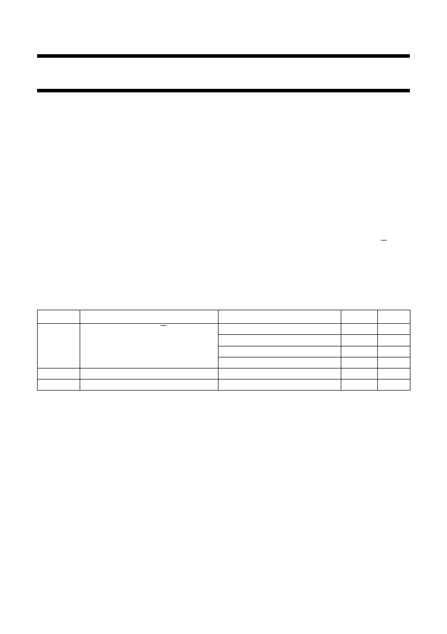
QUICK REFERENCE DATA
GND = 0 V; Tamb =25 °C; tr =tf ≤ 2.5 ns.
Note
1. CPD is used to determine the dynamic power dissipation (PD in W).
PD =CPD × VCC2 × fi +(CL × VCC2 × fo) where:
fi = input frequency in MHz;
fo = output frequency in MHz;
CL = output load capacitance in pF;
VCC = supply voltage in Volts.
SYMBOL
PARAMETER
CONDITIONS
TYPICAL
UNIT
tPHL/tPLH
propagation delay CP to QVCC = 1.8 V; CL = 30 pF; RL =1k
3.4
ns
VCC = 2.5 V; CL = 30 pF; RL = 500
2.3
ns
VCC = 3.3 V; CL = 50 pF; RL = 500
2.4
ns
VCC = 5.0 V; CL = 50 pF; RL = 500
1.8
ns
CI
input capacitance
5
pF
CPD
power dissipation capacitance per buffer
VCC = 3.3 V; notes 1
17
pF
相关PDF资料 |
PDF描述 |
|---|---|
| 0802701R0 | TELEFON-AKKU |
| 935268720115 | LVC/LCX/Z SERIES, 1-BIT DRIVER, TRUE OUTPUT, PDSO5 |
| 935268720118 | LVC/LCX/Z SERIES, 1-BIT DRIVER, TRUE OUTPUT, PDSO5 |
| 935268720125 | LVC/LCX/Z SERIES, 1-BIT DRIVER, TRUE OUTPUT, PDSO5 |
| 935272018125 | LVC/LCX/Z SERIES, 1-BIT DRIVER, TRUE OUTPUT, PDSO5 |
相关代理商/技术参数 |
参数描述 |
|---|---|
| 935272043518 | 制造商:NXP Semiconductors 功能描述:IC SM |
| 935272240128 | 制造商:NXP Semiconductors 功能描述:IC LED DRIVER BLINKER 16-HVQFN |
| 935275527134 | 制造商:NXP Semiconductors 功能描述:IC BUS SWITCH OCTAL QUAD 20TSSOP |
| 935277864112 | 制造商:NXP Semiconductors 功能描述:IC CPU |
| 935278818112 | 制造商:NXP Semiconductors 功能描述:LCD DRVR 20DIGIT 2.5V/3.3V/5V 56-Pin VSO Tube |
发布紧急采购,3分钟左右您将得到回复。