- 您现在的位置:买卖IC网 > PDF目录42411 > 93C46AT-I/OT 128 X 8 MICROWIRE BUS SERIAL EEPROM, PDSO6 PDF资料下载
参数资料
| 型号: | 93C46AT-I/OT |
| 元件分类: | PROM |
| 英文描述: | 128 X 8 MICROWIRE BUS SERIAL EEPROM, PDSO6 |
| 封装: | ROHS COMPLIANT, PLASTIC, SOT-23, 6 PIN |
| 文件页数: | 27/30页 |
| 文件大小: | 548K |
| 代理商: | 93C46AT-I/OT |
第1页第2页第3页第4页第5页第6页第7页第8页第9页第10页第11页第12页第13页第14页第15页第16页第17页第18页第19页第20页第21页第22页第23页第24页第25页第26页当前第27页第28页第29页第30页
93AA46A/B/C, 93LC46A/B/C, 93C46A/B/C
DS21749G-page 6
2008 Microchip Technology Inc.
2.0
FUNCTIONAL DESCRIPTION
When the ORG pin (93XX46C) is connected to VCC,
the (x16) organization is selected. When it is connected
to ground, the (x8) organization is selected. Instruc-
tions, addresses and write data are clocked into the DI
pin on the rising edge of the clock (CLK). The DO pin is
normally held in a High-Z state except when reading
data from the device, or when checking the Ready/
Busy
status during a programming operation. The
Ready/Busy status can be verified during an erase/
write operation by polling the DO pin; DO low indicates
that programming is still in progress, while DO high
indicates the device is ready. DO will enter the High-Z
state on the falling edge of CS.
2.1
Start Condition
The Start bit is detected by the device if CS and DI are
both high with respect to the positive edge of CLK for
the first time.
Before a Start condition is detected, CS, CLK and DI
may change in any combination (except to that of a
Start condition), without resulting in any device
operation (Read, Write, Erase, EWEN, EWDS, ERAL
or WRAL). As soon as CS is high, the device is no
longer in Standby mode.
An instruction following a Start condition will only be
executed if the required opcode, address and data bits
for any particular instruction are clocked in.
2.2
Data In/Data Out (DI/DO)
It is possible to connect the Data In and Data Out pins
together. However, with this configuration it is possible
for a “bus conflict” to occur during the “dummy zero”
that precedes the read operation if A0 is a logic high
level. Under such a condition the voltage level seen at
Data Out is undefined and will depend upon the relative
impedances of Data Out and the signal source driving
A0. The higher the current sourcing capability of A0,
the higher the voltage at the Data Out pin. In order to
limit this current, a resistor should be connected
between DI and DO.
2.3
Data Protection
All modes of operation are inhibited when VCC is below
a typical voltage of 1.5V for ‘93AA’ and ‘93LC’ devices
or 3.8V for ‘93C’ devices.
The EWEN and EWDS commands give additional
protection against accidentally programming during
normal operation.
After power-up, the device is automatically in the
EWDS mode. Therefore, an EWEN instruction must be
performed before the initial ERASE or WRITE instruction
can be executed.
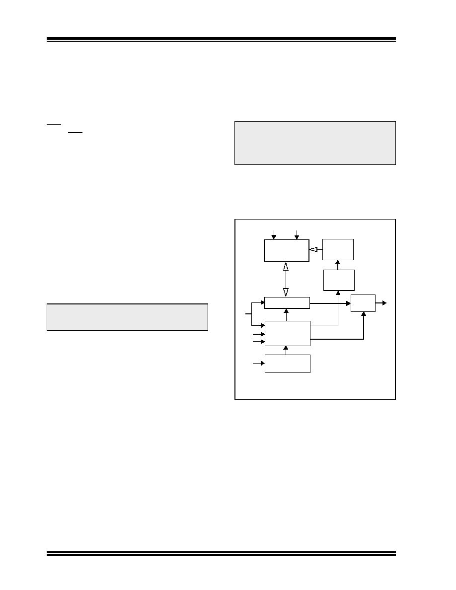
Block Diagram
Note:
When preparing to transmit an instruction,
either the CLK or DI signal levels must be
at a logic low as CS is toggled active high.
Note:
For added protection, an EWDS command
should be performed after every write
operation and an external 10 k
Ω pull-down
protection resistor should be added to the
CS pin.
Memory
Array
Data Register
Mode
Decode
Logic
Clock
Register
Address
Decoder
Address
Counter
Output
Buffer
DO
DI
ORG*
CS
CLK
VCC
VSS
*ORG input is not available on A/B devices
相关PDF资料 |
PDF描述 |
|---|---|
| 93AA46BX-I/SNG | 64 X 16 MICROWIRE BUS SERIAL EEPROM, PDSO8 |
| 93AA46CX-I/MS | 64 X 16 MICROWIRE BUS SERIAL EEPROM, PDSO8 |
| 93LC46A-I/P | 128 X 8 MICROWIRE BUS SERIAL EEPROM, PDIP8 |
| 93LC46CT-I/STG | 64 X 16 MICROWIRE BUS SERIAL EEPROM, PDSO8 |
| 93LC46BXT-I/SNROC | 64 X 16 MICROWIRE BUS SERIAL EEPROM, PDSO8 |
相关代理商/技术参数 |
参数描述 |
|---|---|
| 93C46AX-E/MC | 制造商:MICROCHIP 制造商全称:Microchip Technology 功能描述:1K Microwire Compatible Serial EEPROM |
| 93C46AX-E/MCG | 制造商:MICROCHIP 制造商全称:Microchip Technology 功能描述:1K Microwire Compatible Serial EEPROM |
| 93C46AX-E/MS | 制造商:MICROCHIP 制造商全称:Microchip Technology 功能描述:1K Microwire Compatible Serial EEPROM |
| 93C46AX-E/MSG | 制造商:MICROCHIP 制造商全称:Microchip Technology 功能描述:1K Microwire Compatible Serial EEPROM |
| 93C46AX-E/OT | 制造商:MICROCHIP 制造商全称:Microchip Technology 功能描述:1K Microwire Compatible Serial EEPROM |
发布紧急采购,3分钟左右您将得到回复。