- 您现在的位置:买卖IC网 > PDF目录42444 > 93LC46AT/ST 128 X 8 MICROWIRE BUS SERIAL EEPROM, PDSO8 PDF资料下载
参数资料
| 型号: | 93LC46AT/ST |
| 元件分类: | PROM |
| 英文描述: | 128 X 8 MICROWIRE BUS SERIAL EEPROM, PDSO8 |
| 封装: | TSSOP-8 |
| 文件页数: | 7/12页 |
| 文件大小: | 250K |
| 代理商: | 93LC46AT/ST |
93LC46A/B
DS21173E-page 4
2000 Microchip Technology Inc.
3.0
FUNCTIONAL DESCRIPTION
Instructions, addresses, and write data are clocked into
the DI pin on the rising edge of the clock (CLK). The DO
pin is normally held in a HIGH-Z state except when
reading data from the device, or when checking the
READY/BUSY status during a programming operation.
The READY/BUSY status can be verified during an
ERASE/WRITE operation by polling the DO pin; DO
low indicates that programming is still in progress,
while DO high indicates the device is ready. The DO will
enter the HIGH-Z state on the falling edge of the CS.
3.1
START Condition
The START bit is detected by the device if CS and DI
are both high with respect to the positive edge of CLK
for the first time.
Before a START condition is detected, CS, CLK, and DI
may change in any combination (except to that of a
START condition), without resulting in any device oper-
ation (ERASE, ERAL, EWDS, EWEN, READ, WRITE,
and WRAL). As soon as CS is high, the device is no
longer in the standby mode.
An instruction following a START condition will only be
executed
if
the
required
amount
of
opcodes,
addresses, and data bits for any particular instruction is
clocked in.
After execution of an instruction (i.e., clock in or out of
the last required address or data bit) CLK and DI
become don’t care bits until a new START condition is
detected.
3.2
Data In (DI) and Data Out (DO)
It is possible to connect the Data In (DI) and Data Out
(DO) pins together. However, with this configuration, if
A0 is a logic-high level, it is possible for a “bus conflict”
to occur during the “dummy zero” that precedes the
READ operation. Under such a condition the voltage
level seen at DO is undefined and will depend upon the
relative impedances of DO and the signal source driv-
ing A0. The higher the current sourcing capability of A0,
the higher the voltage at the DO pin.
3.3
Data Protection
During power-up, all programming modes of operation
are inhibited until Vcc has reached a level greater than
2.2V. During power-down, the source data protection
circuitry acts to inhibit all programming modes when
Vcc has fallen below 2.2V at nominal conditions.
The ERASE/WRITE Disable (EWDS) and ERASE/
WRITE Enable (EWDS) commands give additional
protection against accidentally programming during
normal operation.
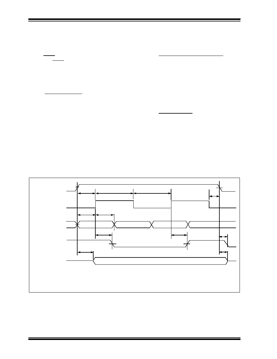
FIGURE 3-1:
SYNCHRONOUS DATA TIMING
CS
VIH
VIL
VIH
VIL
VIH
VIL
VOH
VOL
VOH
VOL
CLK
DI
DO
(READ)
DO
(PROGRAM)
TCSS
TDIS
TCKH
TCKL
TDIH
TPD
TCSH
TPD
TCZ
STATUS VALID
TSV
TCZ
Note:
AC Test Conditions: VIL = 0.4V, VIH = 2.4V
相关PDF资料 |
PDF描述 |
|---|---|
| 93LC46BT/SNROC | 64 X 16 MICROWIRE BUS SERIAL EEPROM, PDSO8 |
| 93LC46BX/SN | 64 X 16 MICROWIRE BUS SERIAL EEPROM, PDSO8 |
| 93LC46BXT/SN | 64 X 16 MICROWIRE BUS SERIAL EEPROM, PDSO8 |
| 93LC46BT/SNA21 | 64 X 16 MICROWIRE BUS SERIAL EEPROM, PDSO8 |
| 93LC46B/SM | 64 X 16 MICROWIRE BUS SERIAL EEPROM, PDSO8 |
相关代理商/技术参数 |
参数描述 |
|---|---|
| 93LC46AX/SN | 功能描述:电可擦除可编程只读存储器 128x8 Rot Pin RoHS:否 制造商:Atmel 存储容量:2 Kbit 组织:256 B x 8 数据保留:100 yr 最大时钟频率:1000 KHz 最大工作电流:6 uA 工作电源电压:1.7 V to 5.5 V 最大工作温度:+ 85 C 安装风格:SMD/SMT 封装 / 箱体:SOIC-8 |
| 93LC46AX-/SN | 制造商:未知厂家 制造商全称:未知厂家 功能描述:Serial EEPROM |
| 93LC46AX-E/MC | 制造商:MICROCHIP 制造商全称:Microchip Technology 功能描述:1K Microwire Compatible Serial EEPROM |
| 93LC46AX-E/MCG | 制造商:MICROCHIP 制造商全称:Microchip Technology 功能描述:1K Microwire Compatible Serial EEPROM |
| 93LC46AX-E/MS | 制造商:MICROCHIP 制造商全称:Microchip Technology 功能描述:1K Microwire Compatible Serial EEPROM |
发布紧急采购,3分钟左右您将得到回复。