- 您现在的位置:买卖IC网 > PDF目录25516 > 954206BGT (INTEGRATED DEVICE TECHNOLOGY INC) 400 MHz, PROC SPECIFIC CLOCK GENERATOR, PDSO56 PDF资料下载
参数资料
| 型号: | 954206BGT |
| 厂商: | INTEGRATED DEVICE TECHNOLOGY INC |
| 元件分类: | 时钟产生/分配 |
| 英文描述: | 400 MHz, PROC SPECIFIC CLOCK GENERATOR, PDSO56 |
| 封装: | 6.10 MM, 0.50 MM PITCH, MO-153N, TSSOP-56 |
| 文件页数: | 8/20页 |
| 文件大小: | 315K |
| 代理商: | 954206BGT |
16
Integrated
Circuit
Systems, Inc.
ICS954206B
Advance Information
0940—06/23/05
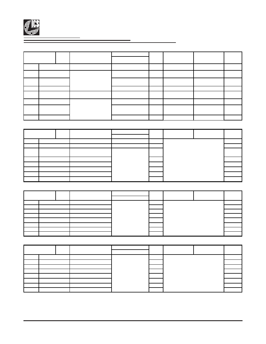
I
2C Table: PEREQ# Control Register
Control
Function
Bit 7
Reserved
RW
0
Bit 6
SATACLK is controlled
RW
1
Bit 5
PCIEX3 is controlled
RW
0
Bit 4
PCIEX1 is controlled
RW
0
Bit 3
Reserved
RW
0
Bit 2
PCIEX4 is controlled
RW
1
Bit 1
PCIEX2 is controlled
RW
0
Bit 0
PCIEX0 is controlled
RW
0
I
2C Table: PLL 2 VCO Frequency Control Register
Control
Function
Bit 7
N Div8
N Divider Prog bit 8
RW
X
Bit 6
N Div9
N Divider Prog bit 9
RW
X
Bit 5
M Div5
RW
X
Bit 4
M Div4
RW
X
Bit 3
M Div3
RW
X
Bit 2
M Div2
RW
X
Bit 1
M Div1
RW
X
Bit 0
M Div0
RW
X
I
2C Table: PLL 2 VCO Frequency Control Register
Control
Function
Bit 7
N Div7
RW
X
Bit 6
N Div6
RW
X
Bit 5
N Div5
RW
X
Bit 4
N Div4
RW
X
Bit 3
N Div3
RW
X
Bit 2
N Div2
RW
X
Bit 1
N Div1
RW
X
Bit 0
N Div0
RW
X
I
2C Table: PLL 2 Spread Spectrum Control Register
Control
Function
Bit 7
SSP7
RW
X
Bit 6
SSP6
RW
X
Bit 5
SSP5
RW
X
Bit 4
SSP4
RW
X
Bit 3
SSP3
RW
X
Bit 2
SSP2
RW
X
Bit 1
SSP1
RW
X
Bit 0
SSP0
RW
X
--
1
Not Controlled
Controlled
1
The decimal representation of M and N
Divier in Byte 17 and 18 will configure the
VCO frequency. Default at power up =
Byte 0 Rom table. VCO Frequency =
14.318 x [NDiv(9:0)+8] / [MDiv(5:0)+2]
The decimal representation of M and N
Divier in Byte 17 and 18 will configure the
VCO frequency. Default at power up =
Byte 0 Rom table. VCO Frequency =
14.318 x [NDiv(9:0)+8] / [MDiv(5:0)+2]
Controlled
Not Controlled
Controlled
Not Controlled
Name
Type
M Divider Programming
bits
Type
-
Byte 19
Pin #
Spread Spectrum
Programming b(7:0)
These Spread Spectrum bits in Byte 19
and 20 will program the spread
pecentage. It is recommended to use
ICS Spread % table for spread
programming.
PWD
01
PWD
0
PWD
Name
Type
0
1
Pin #
Byte 16
-
Type
-
Pin #
Name
PEREQ2# controls selected
outputs. Outputs controlled
by this pin will be Hi-Z when
PEREQ2# is high.
PEREQ1# controls selected
outputs. Outputs controlled
by this pin will be Hi-Z when
PEREQ1# is high.
-
Byte 17
-
N Divider Programming
b(8:0)
-
Byte 18
Pin #
Name
-
Controlled
-
Not Controlled
-
相关PDF资料 |
PDF描述 |
|---|---|
| 954206BFT | 400 MHz, PROC SPECIFIC CLOCK GENERATOR, PDSO56 |
| 954206BFLFT | 400 MHz, PROC SPECIFIC CLOCK GENERATOR, PDSO56 |
| 9552-6006-01 | RF/MICROWAVE FIXED ATTENUATOR |
| 9552-6006-03 | RF/MICROWAVE FIXED ATTENUATOR |
| 9552-6006-04 | RF/MICROWAVE FIXED ATTENUATOR |
相关代理商/技术参数 |
参数描述 |
|---|---|
| 9-5-421 | 功能描述:3M 421 LEAD FOIL TAPE - 9" X 5YD 制造商:3m (tc) 系列:421 零件状态:在售 标准包装:1 |
| 954213AGLF | 制造商:Integrated Device Technology Inc 功能描述:PROGRAMMABLE TIMING CONTROL HUB FOR MOBILE P4 SYSTEMS |
| 954213AGLFT | 制造商:Integrated Device Technology Inc 功能描述:PROGRAMMABLE TIMING CONTROL HUB FOR MOBILE P4 SYSTEMS |
| 954217AGLF | 制造商:Integrated Device Technology Inc 功能描述: |
| 954217AGLFT | 制造商:Integrated Device Technology Inc 功能描述: |
发布紧急采购,3分钟左右您将得到回复。