- 您现在的位置:买卖IC网 > PDF目录25548 > 97U877AKLF-T (INTEGRATED DEVICE TECHNOLOGY INC) 97U SERIES, PLL BASED CLOCK DRIVER, 10 TRUE OUTPUT(S), 0 INVERTED OUTPUT(S), QCC40 PDF资料下载
参数资料
| 型号: | 97U877AKLF-T |
| 厂商: | INTEGRATED DEVICE TECHNOLOGY INC |
| 元件分类: | 时钟及定时 |
| 英文描述: | 97U SERIES, PLL BASED CLOCK DRIVER, 10 TRUE OUTPUT(S), 0 INVERTED OUTPUT(S), QCC40 |
| 封装: | MLF-40 |
| 文件页数: | 6/13页 |
| 文件大小: | 1125K |
| 代理商: | 97U877AKLF-T |
2
ICS97U877AHLF/AKLF
Advance Information
0792—12/18/03
Pin Descriptions
l
a
n
i
m
r
e
T
e
m
a
N
n
o
i
t
p
i
r
c
s
e
D
l
a
c
i
r
t
c
e
l
E
s
c
i
t
s
i
r
e
t
c
a
r
a
h
C
D
N
G
Ad
n
u
o
r
G
g
o
l
a
n
A
d
n
u
o
r
G
V
A
D
r
e
w
o
p
g
o
l
a
n
A
l
a
n
i
m
o
n
V
8
.
1
T
N
I
_
K
L
Cr
o
t
s
i
s
e
r
n
w
o
d
l
u
p
)
m
h
O
K
0
1
-
K
0
1
(
a
h
t
i
w
t
u
p
n
i
k
c
o
l
C
t
u
p
n
i
l
a
i
t
n
e
r
e
f
i
D
C
N
I
_
K
L
C
r
o
t
s
i
s
e
r
n
w
o
d
l
u
p
)
m
h
O
K
0
1
-
K
0
1
(
a
h
t
i
w
t
u
p
n
i
k
c
o
l
c
y
r
a
t
n
e
l
p
m
o
C
t
u
p
n
i
l
a
i
t
n
e
r
e
f
i
D
T
N
I
_
B
Ft
u
p
n
i
k
c
o
l
c
k
c
a
b
d
e
F
t
u
p
n
i
l
a
i
t
n
e
r
e
f
i
D
C
N
I
_
B
Ft
u
p
n
i
k
c
o
l
c
k
c
a
b
d
e
f
y
r
a
t
n
e
m
e
l
p
m
o
C
t
u
p
n
i
l
a
i
t
n
e
r
e
f
i
D
T
U
O
_
B
Ft
u
p
t
u
o
k
c
o
l
c
k
c
a
b
d
e
F
t
u
p
t
u
o
l
a
i
t
n
e
r
e
f
i
D
C
T
U
O
_
B
Ft
u
p
t
u
o
k
c
o
l
c
k
c
a
b
d
e
f
y
r
a
t
n
e
m
e
l
p
m
o
C
t
u
p
t
u
o
l
a
i
t
n
e
r
e
f
i
D
E
O)
s
u
o
n
o
r
h
c
n
y
s
A
(
e
l
b
a
n
E
t
u
p
t
u
O
t
u
p
n
i
S
O
M
C
V
L
S
OV
r
o
D
N
G
o
t
d
e
i
t
(
t
c
e
l
e
S
t
u
p
t
u
O
Q
D
)t
u
p
n
i
S
O
M
C
V
L
D
N
Gd
n
u
o
r
G
d
n
u
o
r
G
V
Q
D
r
e
w
o
p
t
u
p
t
u
o
d
n
a
c
i
g
o
L
l
a
n
i
m
o
n
V
8
.
1
]
9
:
0
[
T
K
L
Cs
t
u
p
t
u
o
k
c
o
l
C
s
t
u
p
t
u
o
l
a
i
t
n
e
r
e
f
i
D
]
9
:
0
[
C
K
L
Cs
t
u
p
t
u
o
k
c
o
l
c
y
r
a
t
n
e
m
e
l
p
m
o
C
s
t
u
p
t
u
o
l
a
i
t
n
e
r
e
f
i
D
B
Nll
a
b
o
N
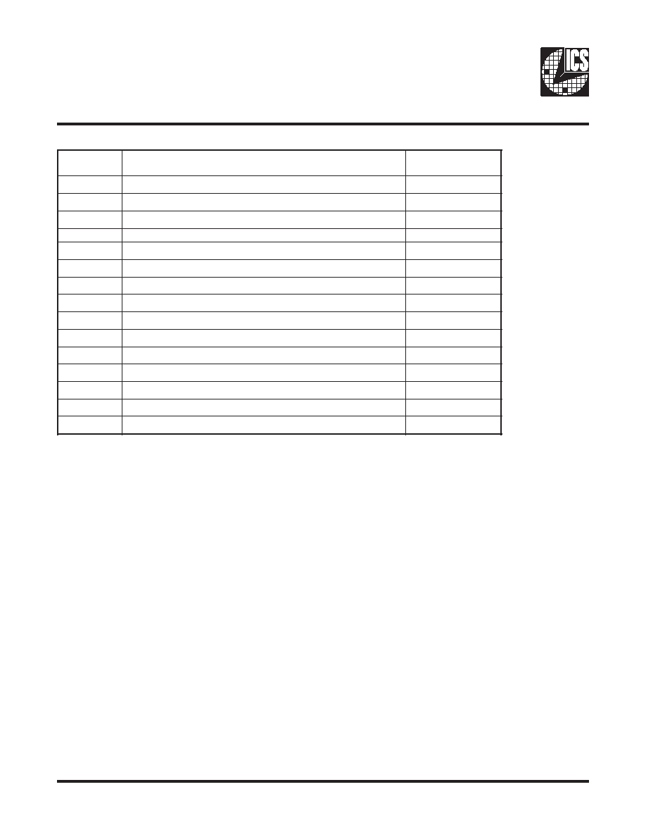
The PLL clock buffer, ICS97U877, is designed for a VDDQ of 1.8 V, a AVDD of 1.8 V and differential data input and output
levels. Package options include a plastic 52-ball VFBGA and a 40-pin MLF.
ICS97U877 is a zero delay buffer that distributes a differential clock input pair (CLK_INT, CLK_INC) to ten differential
pair of clock outputs (CLKT[0:9], CLKC[0:9]) and one differential pair feedback clock outputs (FB_OUTT, FBOUTC).
The clock outputs are controlled by the input clocks (CLK_INT, CLK_INC), the feedback clocks (FB_INT, FB_INC), the
LVCMOS program pins (OE, OS) and the Analog Power input (AVDD).When OE is low, the outputs (except FB_OUTT/
FB_OUTC) are disabled while the internal PLL continues to maintain its locked-in frequency. OS (Output Select) is a
program pin that must be tied to GND or VDDQ.When OS is high, OE will function as described above.When OS is low,
OE has no effect on CLKT7/CLKC7 (they are free running in addition to FB_OUTT/FB_OUTC).When AVDD is grounded,
the PLL is turned off and bypassed for test purposes.
When both clock signals (CLK_INT, CLK_INC) are logic low, the device will enter a low power mode. An input logic
detection circuit on the differential inputs, independent from the input buffers, will detect the logic low level and perform
a low power state where all outputs, the feedback and the PLL are OFF.When the inputs transition from both being logic
low to being differential signals, the PLL will be turned back on, the inputs and outputs will be enabled and the PLL
will obtain phase lock between the feedback clock pair (FB_INT, FB_INC) and the input clock pair (CLK_INT, CLK_INC)
within the specified stabilization time tSTAB.
The PLL in ICS97U877 clock driver uses the input clocks (CLK_INT, CLK_INC) and the feedback clocks (FB_INT,
FB_INC) to provide high-performance, low-skew, low-jitter output differential clocks (CLKT[0:9], CLKC[0:9]). ICS97U877
is also able to track Spread Spectrum Clocking (SSC) for reduced EMI.
ICS97U877 is characterized for operation from 0°C to 70°C.
相关PDF资料 |
PDF描述 |
|---|---|
| 97U877AHT | 97U SERIES, PLL BASED CLOCK DRIVER, 10 TRUE OUTPUT(S), 0 INVERTED OUTPUT(S), PBGA52 |
| 97U877AH | 97U SERIES, PLL BASED CLOCK DRIVER, 10 TRUE OUTPUT(S), 0 INVERTED OUTPUT(S), PBGA52 |
| 97U877AKT | 97U SERIES, PLL BASED CLOCK DRIVER, 10 TRUE OUTPUT(S), 0 INVERTED OUTPUT(S), PQCC40 |
| 97U877AHLF | 97U SERIES, PLL BASED CLOCK DRIVER, 10 TRUE OUTPUT(S), 0 INVERTED OUTPUT(S), PBGA52 |
| 97U877YK-T | 97U SERIES, PLL BASED CLOCK DRIVER, 10 TRUE OUTPUT(S), 0 INVERTED OUTPUT(S), PQCC40 |
相关代理商/技术参数 |
参数描述 |
|---|---|
| 97ULP844AH | 功能描述:时钟驱动器及分配 RoHS:否 制造商:Micrel 乘法/除法因子:1:4 输出类型:Differential 最大输出频率:4.2 GHz 电源电压-最大: 电源电压-最小:5 V 最大工作温度:+ 85 C 封装 / 箱体:SOIC-8 封装:Reel |
| 97ULP844AHLF | 功能描述:时钟驱动器及分配 RoHS:否 制造商:Micrel 乘法/除法因子:1:4 输出类型:Differential 最大输出频率:4.2 GHz 电源电压-最大: 电源电压-最小:5 V 最大工作温度:+ 85 C 封装 / 箱体:SOIC-8 封装:Reel |
| 97ULP844AHLFT | 功能描述:时钟驱动器及分配 RoHS:否 制造商:Micrel 乘法/除法因子:1:4 输出类型:Differential 最大输出频率:4.2 GHz 电源电压-最大: 电源电压-最小:5 V 最大工作温度:+ 85 C 封装 / 箱体:SOIC-8 封装:Reel |
| 97ULP844AHT | 功能描述:时钟驱动器及分配 RoHS:否 制造商:Micrel 乘法/除法因子:1:4 输出类型:Differential 最大输出频率:4.2 GHz 电源电压-最大: 电源电压-最小:5 V 最大工作温度:+ 85 C 封装 / 箱体:SOIC-8 封装:Reel |
| 97ULP845AH | 功能描述:时钟驱动器及分配 RoHS:否 制造商:Micrel 乘法/除法因子:1:4 输出类型:Differential 最大输出频率:4.2 GHz 电源电压-最大: 电源电压-最小:5 V 最大工作温度:+ 85 C 封装 / 箱体:SOIC-8 封装:Reel |
发布紧急采购,3分钟左右您将得到回复。