- 您现在的位置:买卖IC网 > PDF目录25564 > 9DB403DFLF (INTEGRATED DEVICE TECHNOLOGY INC) 9DB SERIES, PLL BASED CLOCK DRIVER, 4 TRUE OUTPUT(S), 0 INVERTED OUTPUT(S), PDSO28 PDF资料下载
参数资料
| 型号: | 9DB403DFLF |
| 厂商: | INTEGRATED DEVICE TECHNOLOGY INC |
| 元件分类: | 时钟及定时 |
| 英文描述: | 9DB SERIES, PLL BASED CLOCK DRIVER, 4 TRUE OUTPUT(S), 0 INVERTED OUTPUT(S), PDSO28 |
| 封装: | 0.209 INCH, ROHS COMPLIANT, MO-150, SSOP-28 |
| 文件页数: | 6/19页 |
| 文件大小: | 194K |
| 代理商: | 9DB403DFLF |
IDTTM/ICSTM
Four Output Differential Buffer for PCIe Gen 1 and Gen 2
ICS9DB403D
REV N 05/09/11
ICS9DB403D
Four Output Differential Buffer for PCIe for Gen 1 and Gen 2
14
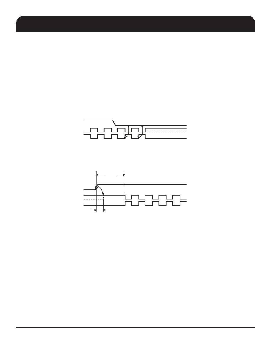
The PD# pin cleanly shuts off all clocks and places the device into a power saving mode. PD# must be asserted before shutting
off the input clock or power to insure an orderly shutdown. PD is asynchronous active-low input for both powering down the
device and powering up the device. When PD# is asserted, all clocks will be driven high, or tri-stated (depending on the PD#
drive mode and Output control bits) before the PLL is shut down.
PD#, Power Down
When PD# is sampled low by two consecutive rising edges of DIF#, all DIF outputs must be held High, or tri-stated (depending
on the PD# drive mode and Output control bits) on the next High-Low transition of the DIF# outputs. When the PD# drive mode
bit is set to ‘0’, all clock outputs will be held with DIF driven High with 2 x IREF and DIF# tri-stated. If the PD# drive mode bit is
set to ‘1’, both DIF and DIF# are tri-stated.
PD# Assertion
Power-up latency is less than 1 ms. This is the time from de-assertion of the PD# pin, or VDD reaching 3.3V, or the time from
valid SRC_IN clocks until the time that stable clocks are output from the device (PLL Locked). If the PD# drive mode bit is set
to ‘1’, all the DIF outputs must driven to a voltage of >200 mV within 300 us of PD# de-assertion.
PD# De-assertion
PWRDWN#
DIF
DIF#
PWRDWN#
DIF
DIF#
Tstable
<1mS
Tdrive_PwrDwn#
<300uS, >200mV
Note: Polarities in timing diagrams are shown OE_INV = 0. They are similar to OE_INV = 1.
相关PDF资料 |
PDF描述 |
|---|---|
| 9DB423BFLFT | 9DB SERIES, PLL BASED CLOCK DRIVER, 4 TRUE OUTPUT(S), 0 INVERTED OUTPUT(S), PDSO28 |
| 9DB423BFLF | 9DB SERIES, PLL BASED CLOCK DRIVER, 4 TRUE OUTPUT(S), 0 INVERTED OUTPUT(S), PDSO28 |
| 9DB433AFILFT | 9DB SERIES, PLL BASED CLOCK DRIVER, 4 TRUE OUTPUT(S), 0 INVERTED OUTPUT(S), PDSO28 |
| 9DB433AFLF | 9DB SERIES, PLL BASED CLOCK DRIVER, 4 TRUE OUTPUT(S), 0 INVERTED OUTPUT(S), PDSO28 |
| 9DB433AFLIFT | 9DB SERIES, PLL BASED CLOCK DRIVER, 4 TRUE OUTPUT(S), 0 INVERTED OUTPUT(S), PDSO28 |
相关代理商/技术参数 |
参数描述 |
|---|---|
| 9DB403DFLFT | 功能描述:时钟缓冲器 4 OUTPUT PCIE GEN1 BUFFER RoHS:否 制造商:Texas Instruments 输出端数量:5 最大输入频率:40 MHz 传播延迟(最大值): 电源电压-最大:3.45 V 电源电压-最小:2.375 V 最大功率耗散: 最大工作温度:+ 85 C 最小工作温度:- 40 C 封装 / 箱体:LLP-24 封装:Reel |
| 9DB403DGILF | 功能描述:时钟缓冲器 4 OUTPUT PCIE GEN1 BUFFER RoHS:否 制造商:Texas Instruments 输出端数量:5 最大输入频率:40 MHz 传播延迟(最大值): 电源电压-最大:3.45 V 电源电压-最小:2.375 V 最大功率耗散: 最大工作温度:+ 85 C 最小工作温度:- 40 C 封装 / 箱体:LLP-24 封装:Reel |
| 9DB403DGILFT | 功能描述:时钟缓冲器 4 OUTPUT PCIE GEN1 BUFFER RoHS:否 制造商:Texas Instruments 输出端数量:5 最大输入频率:40 MHz 传播延迟(最大值): 电源电压-最大:3.45 V 电源电压-最小:2.375 V 最大功率耗散: 最大工作温度:+ 85 C 最小工作温度:- 40 C 封装 / 箱体:LLP-24 封装:Reel |
| 9DB403DGLF | 功能描述:时钟缓冲器 4 OUTPUT PCIE GEN1 BUFFER RoHS:否 制造商:Texas Instruments 输出端数量:5 最大输入频率:40 MHz 传播延迟(最大值): 电源电压-最大:3.45 V 电源电压-最小:2.375 V 最大功率耗散: 最大工作温度:+ 85 C 最小工作温度:- 40 C 封装 / 箱体:LLP-24 封装:Reel |
| 9DB403DGLFT | 功能描述:时钟缓冲器 4 OUTPUT PCIE GEN1 BUFFER RoHS:否 制造商:Texas Instruments 输出端数量:5 最大输入频率:40 MHz 传播延迟(最大值): 电源电压-最大:3.45 V 电源电压-最小:2.375 V 最大功率耗散: 最大工作温度:+ 85 C 最小工作温度:- 40 C 封装 / 箱体:LLP-24 封装:Reel |
发布紧急采购,3分钟左右您将得到回复。