- 您现在的位置:买卖IC网 > PDF目录25564 > 9DB423BFLF (INTEGRATED DEVICE TECHNOLOGY INC) 9DB SERIES, PLL BASED CLOCK DRIVER, 4 TRUE OUTPUT(S), 0 INVERTED OUTPUT(S), PDSO28 PDF资料下载
参数资料
| 型号: | 9DB423BFLF |
| 厂商: | INTEGRATED DEVICE TECHNOLOGY INC |
| 元件分类: | 时钟及定时 |
| 英文描述: | 9DB SERIES, PLL BASED CLOCK DRIVER, 4 TRUE OUTPUT(S), 0 INVERTED OUTPUT(S), PDSO28 |
| 封装: | 0.209 INCH, ROHS COMPLIANT, MO-150, SSOP-28 |
| 文件页数: | 13/19页 |
| 文件大小: | 199K |
| 代理商: | 9DB423BFLF |
IDT
Four Output Differential Buffer for PCIe Gen 1, Gen 2 and QPI
1437 Rev D - 05/09/11
9DB423B
Four Output Differential Buffer for PCIe for Gen 1, Gen 2 and QPI
3
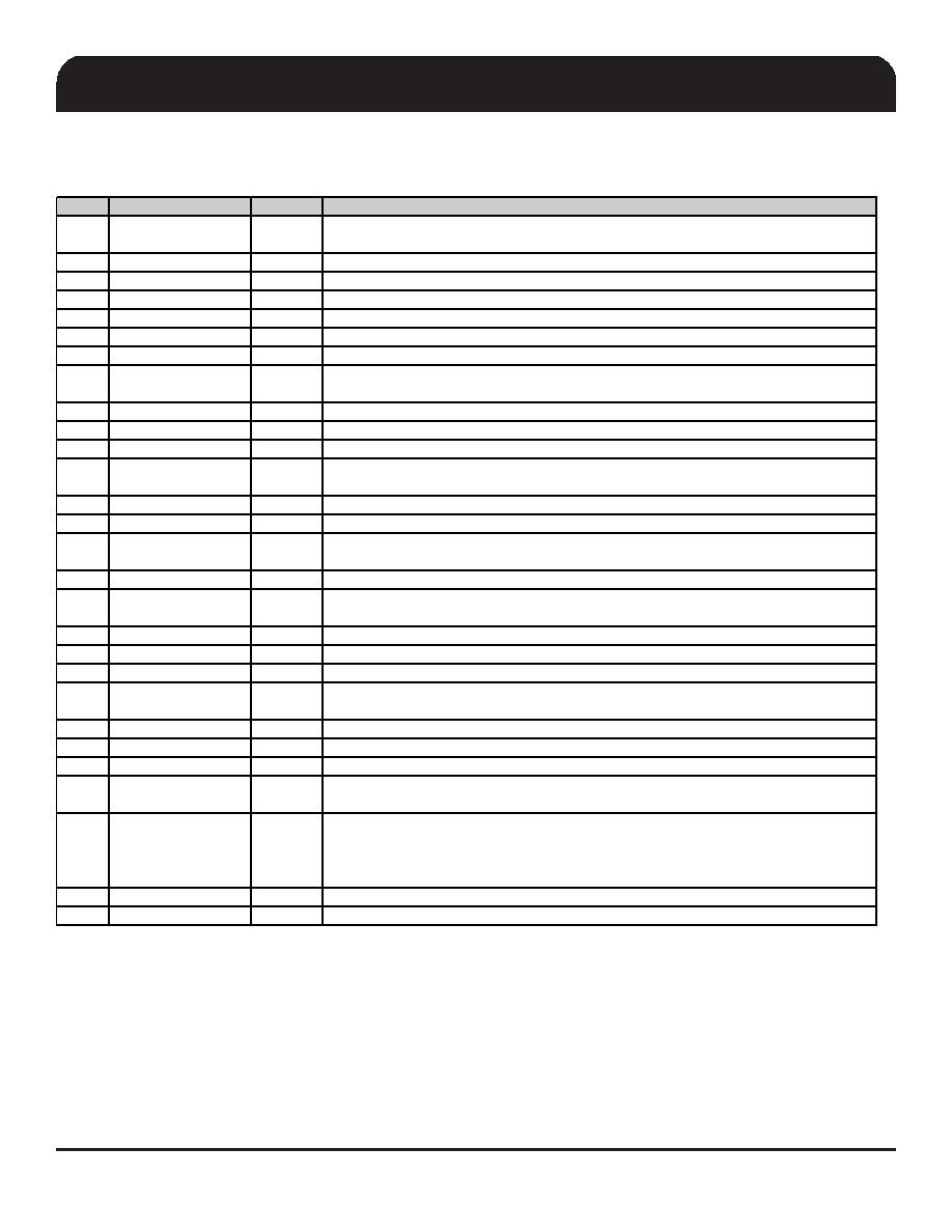
Pin Description for OE_INV = 0
PIN #
PIN NAME
PIN TYPE
DESCRIPTION
1VDDR
PWR
3.3V power for differential input clock (receiver). This VDD should be treated as an
analog power rail and filtered appropriately.
2
SRC_IN
IN
0.7 V Differential SRC TRUE input
3
SRC_IN#
IN
0.7 V Differential SRC COMPLEMENTARY input
4
GND
PWR
Ground pin.
5
VDD
PWR
Power supply, nominal 3.3V
6
DIF_1
OUT
0.7V differential true clock output
7
DIF_1#
OUT
0.7V differential Complementary clock output
8OE_1
IN
Active high input for enabling output 1.
0 =disable outputs, 1= enable outputs
9
DIF_2
OUT
0.7V differential true clock output
10
DIF_2#
OUT
0.7V differential Complementary clock output
11
VDD
PWR
Power supply, nominal 3.3V
12
BYPASS#_133_100
IN
Input to select Bypass(fan-out), QPI PLL (133MHz) or PCIe PLL (100MHz) mode
0 = Bypass mode, M= QPI, 1= PCIe PLL mode
13
SCLK
IN
Clock pin of SMBus circuitry, 5V tolerant.
14
SDATA
I/O
Data pin for SMBus circuitry, 5V tolerant.
15
PD#
IN
Asynchronous active low input pin used to power down the device. The internal
clocks are disabled and the VCO and the crystal osc. (if any) are stopped.
16
DIF_STOP#
IN
Active low input to stop differential output clocks.
17
HIGH_BW#
IN
3.3V input for selecting PLL Band Width
0 = High, 1= Low
18
VDD
PWR
Power supply, nominal 3.3V
19
DIF_5#
OUT
0.7V differential Complementary clock output
20
DIF_5
OUT
0.7V differential true clock output
21
OE_6
IN
Active high input for enabling output 6.
0 =disable outputs, 1= enable outputs
22
DIF_6#
OUT
0.7V differential Complementary clock output
23
DIF_6
OUT
0.7V differential true clock output
24
VDD
PWR
Power supply, nominal 3.3V
25
OE_INV
IN
This latched input selects the polarity of the OE pins.
0 = OE pins active high, 1 = OE pins active low (OE#)
26
IREF
OUT
This pin establishes the reference for the differential current-mode output pairs. It
requires a fixed precision resistor to ground. 475ohm is the standard value for
100ohm differential impedance. Other impedances require different values. See data
sheet.
27
GNDA
PWR
Ground pin for the PLL core.
28
VDDA
PWR
3.3V power for the PLL core.
相关PDF资料 |
PDF描述 |
|---|---|
| 9DB433AFILFT | 9DB SERIES, PLL BASED CLOCK DRIVER, 4 TRUE OUTPUT(S), 0 INVERTED OUTPUT(S), PDSO28 |
| 9DB433AFLF | 9DB SERIES, PLL BASED CLOCK DRIVER, 4 TRUE OUTPUT(S), 0 INVERTED OUTPUT(S), PDSO28 |
| 9DB433AFLIFT | 9DB SERIES, PLL BASED CLOCK DRIVER, 4 TRUE OUTPUT(S), 0 INVERTED OUTPUT(S), PDSO28 |
| 9DB433AGILFT | 9DB SERIES, PLL BASED CLOCK DRIVER, 4 TRUE OUTPUT(S), 0 INVERTED OUTPUT(S), PDSO28 |
| 9DB433AFLFT | 9DB SERIES, PLL BASED CLOCK DRIVER, 4 TRUE OUTPUT(S), 0 INVERTED OUTPUT(S), PDSO28 |
相关代理商/技术参数 |
参数描述 |
|---|---|
| 9DB423BFLFT | 功能描述:外围驱动器与原件 - PCI 4 OUTPUT PCIE GEN2 BUFFER w/QPI RoHS:否 制造商:PLX Technology 工作电源电压: 最大工作温度: 安装风格:SMD/SMT 封装 / 箱体:FCBGA-1156 封装:Tray |
| 9DB423BGLF | 功能描述:时钟缓冲器 4 OUTPUT PCIE GEN2 BUFFER w/QPI RoHS:否 制造商:Texas Instruments 输出端数量:5 最大输入频率:40 MHz 传播延迟(最大值): 电源电压-最大:3.45 V 电源电压-最小:2.375 V 最大功率耗散: 最大工作温度:+ 85 C 最小工作温度:- 40 C 封装 / 箱体:LLP-24 封装:Reel |
| 9DB423BGLFT | 功能描述:时钟缓冲器 4 OUTPUT PCIE GEN2 BUFFER w/QPI RoHS:否 制造商:Texas Instruments 输出端数量:5 最大输入频率:40 MHz 传播延迟(最大值): 电源电压-最大:3.45 V 电源电压-最小:2.375 V 最大功率耗散: 最大工作温度:+ 85 C 最小工作温度:- 40 C 封装 / 箱体:LLP-24 封装:Reel |
| 9DB433AFILF | 功能描述:时钟缓冲器 4 OUTPUT PCIE GEN3 BUFFER RoHS:否 制造商:Texas Instruments 输出端数量:5 最大输入频率:40 MHz 传播延迟(最大值): 电源电压-最大:3.45 V 电源电压-最小:2.375 V 最大功率耗散: 最大工作温度:+ 85 C 最小工作温度:- 40 C 封装 / 箱体:LLP-24 封装:Reel |
| 9DB433AFILFT | 功能描述:时钟缓冲器 4 OUTPUT PCIE GEN3 BUFFER RoHS:否 制造商:Texas Instruments 输出端数量:5 最大输入频率:40 MHz 传播延迟(最大值): 电源电压-最大:3.45 V 电源电压-最小:2.375 V 最大功率耗散: 最大工作温度:+ 85 C 最小工作温度:- 40 C 封装 / 箱体:LLP-24 封装:Reel |
发布紧急采购,3分钟左右您将得到回复。