- 您现在的位置:买卖IC网 > PDF目录25564 > 9DB433AGILFT (INTEGRATED DEVICE TECHNOLOGY INC) 9DB SERIES, PLL BASED CLOCK DRIVER, 4 TRUE OUTPUT(S), 0 INVERTED OUTPUT(S), PDSO28 PDF资料下载
参数资料
| 型号: | 9DB433AGILFT |
| 厂商: | INTEGRATED DEVICE TECHNOLOGY INC |
| 元件分类: | 时钟及定时 |
| 英文描述: | 9DB SERIES, PLL BASED CLOCK DRIVER, 4 TRUE OUTPUT(S), 0 INVERTED OUTPUT(S), PDSO28 |
| 封装: | 4.40 MM, 0.65 MM PITCH, ROHS COMPLIANT, MO-153, TSSOP-28 |
| 文件页数: | 3/16页 |
| 文件大小: | 190K |
| 代理商: | 9DB433AGILFT |
IDT
Four Output Differential Buffer for PCIe Gen 3
1658B - 05/09/11
9DB433
Four Output Differential Buffer for PCIe Gen 3
11
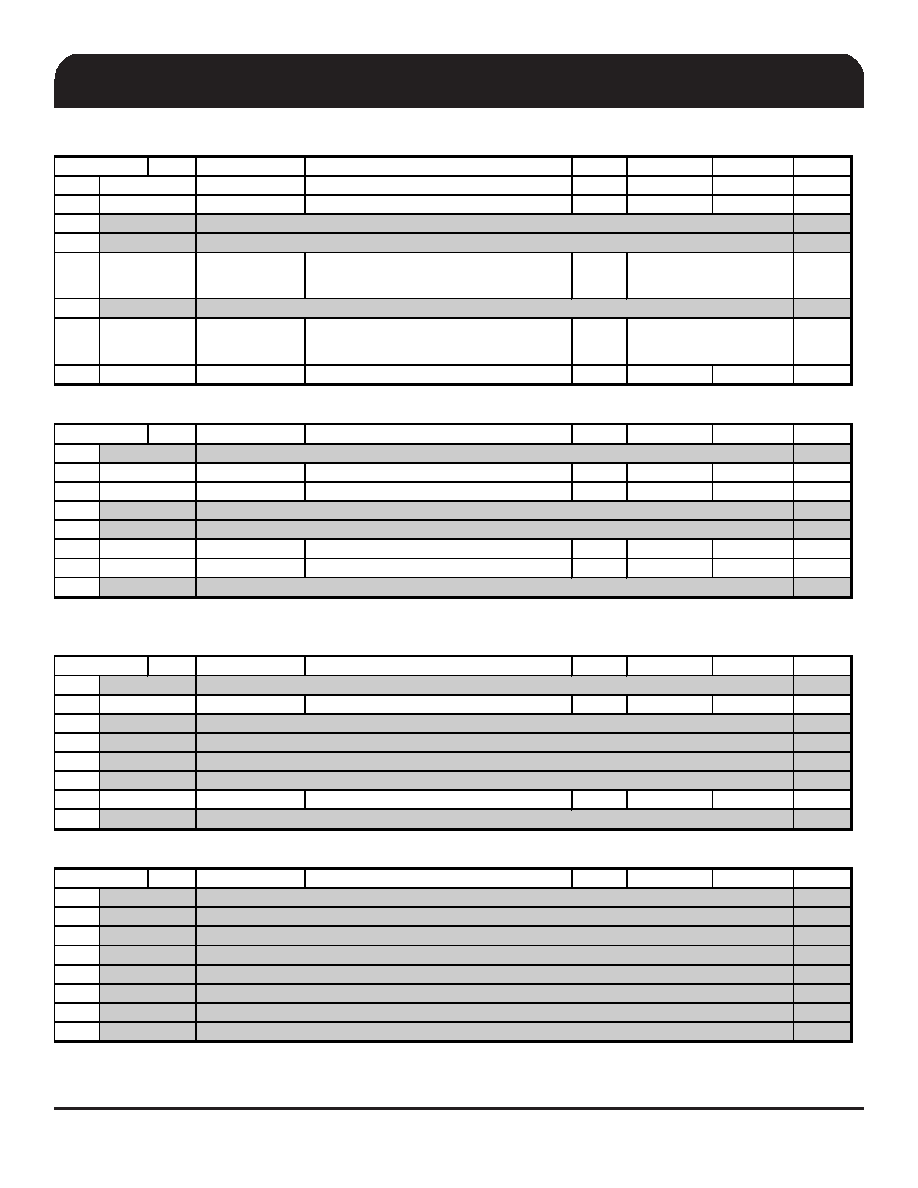
SMBus Table: Frequency Select Register, READ/WRITE ADDRESS (Selectable)
Pin #
Name
Control Function
Type
0
1
Default
Bit 7
PD_Mode
PD# drive mode
RW
driven
Hi-Z
1
Bit 6
OE_Mode
OE#_Stop drive mode
RW
driven
Hi-Z
0
Bit 5
0
Bit 4
X
Bit 3
MODE1
BYPASS#/PLL1
RW
Input
Bit 2
1
Bit 1
MODE0
BYPASS#/PLL0
RW
Input
Bit 0
SRC_DIV#
SRC Divide by 2 Select
RW
x/2
x/1
1
SMBus Table: Output Control Register
Pin #
Name
Control Function
Type
0
1
Default
Bit 7
1
Bit 6
DIF_6
Output Enable
RW
Disable
Enable
1
Bit 5
DIF_5
Output Enable
RW
Disable
Enable
1
Bit 4
1
Bit 3
1
Bit 2
DIF_2
Output Enable
RW
Disable
Enable
1
Bit 1
DIF_1
Output Enable
RW
Disable
Enable
1
Bit 0
1
NOTE: The SMBus Output Enable Bit must be '1' AND the respective OE pin must be active for the output to run!
SMBus Table: OE Pin Control Register
Pin #
Name
Control Function
Type
0
1
Default
Bit 7
0
Bit 6
DIF_6
DIF_6 Stoppable with OE6#
RW
Free-run
Stoppable
0
Bit 5
0
Bit 4
0
Bit 3
0
Bit 2
0
Bit 1
DIF_1
DIF_1 Stoppable with OE1#
RW
Free-run
Stoppable
0
Bit 0
0
SMBus Table: Reserved Register
Pin #
Name
Control Function
Type
0
1
Default
Bit 7
X
Bit 6
X
Bit 5
X
Bit 4
X
Bit 3
X
Bit 2
X
Bit 1
X
Bit 0
X
Reserved
Byte 3
Reserved
6,7
Byte 2
22,23
9,10
6,7
Byte 1
22,23
19,20
Byte 0
-
See Operating Mode
Readback Table
See Operating Mode
Readback Table
Reserved
相关PDF资料 |
PDF描述 |
|---|---|
| 9DB433AFLFT | 9DB SERIES, PLL BASED CLOCK DRIVER, 4 TRUE OUTPUT(S), 0 INVERTED OUTPUT(S), PDSO28 |
| 9DB633AFLIFT | 9DB SERIES, PLL BASED CLOCK DRIVER, 6 TRUE OUTPUT(S), 0 INVERTED OUTPUT(S), PDSO28 |
| 9DB633AGILF | 9DB SERIES, PLL BASED CLOCK DRIVER, 6 TRUE OUTPUT(S), 0 INVERTED OUTPUT(S), PDSO28 |
| 9DB633AFLFT | 9DB SERIES, PLL BASED CLOCK DRIVER, 6 TRUE OUTPUT(S), 0 INVERTED OUTPUT(S), PDSO28 |
| 9DB633AGILFT | 9DB SERIES, PLL BASED CLOCK DRIVER, 6 TRUE OUTPUT(S), 0 INVERTED OUTPUT(S), PDSO28 |
相关代理商/技术参数 |
参数描述 |
|---|---|
| 9DB433AGLF | 功能描述:时钟缓冲器 4 OUTPUT PCIE GEN3 BUFFER RoHS:否 制造商:Texas Instruments 输出端数量:5 最大输入频率:40 MHz 传播延迟(最大值): 电源电压-最大:3.45 V 电源电压-最小:2.375 V 最大功率耗散: 最大工作温度:+ 85 C 最小工作温度:- 40 C 封装 / 箱体:LLP-24 封装:Reel |
| 9DB433AGLFT | 功能描述:时钟缓冲器 4 OUTPUT PCIE GEN3 BUFFER RoHS:否 制造商:Texas Instruments 输出端数量:5 最大输入频率:40 MHz 传播延迟(最大值): 电源电压-最大:3.45 V 电源电压-最小:2.375 V 最大功率耗散: 最大工作温度:+ 85 C 最小工作温度:- 40 C 封装 / 箱体:LLP-24 封装:Reel |
| 9DB633 | 制造商:IDT 制造商全称:Integrated Device Technology 功能描述:Six Output Differential Buffer for PCIe Gen3 |
| 9DB633AFILF | 功能描述:时钟缓冲器 4 OUTPUT PCIE GEN3 BUFFER RoHS:否 制造商:Texas Instruments 输出端数量:5 最大输入频率:40 MHz 传播延迟(最大值): 电源电压-最大:3.45 V 电源电压-最小:2.375 V 最大功率耗散: 最大工作温度:+ 85 C 最小工作温度:- 40 C 封装 / 箱体:LLP-24 封装:Reel |
| 9DB633AFILFT | 功能描述:时钟缓冲器 4 OUTPUT PCIE GEN3 BUFFER RoHS:否 制造商:Texas Instruments 输出端数量:5 最大输入频率:40 MHz 传播延迟(最大值): 电源电压-最大:3.45 V 电源电压-最小:2.375 V 最大功率耗散: 最大工作温度:+ 85 C 最小工作温度:- 40 C 封装 / 箱体:LLP-24 封装:Reel |
发布紧急采购,3分钟左右您将得到回复。