- 您现在的位置:买卖IC网 > PDF目录25565 > 9DBL411AKLFT (INTEGRATED DEVICE TECHNOLOGY INC) LOW SKEW CLOCK DRIVER, PQCC20 PDF资料下载
参数资料
| 型号: | 9DBL411AKLFT |
| 厂商: | INTEGRATED DEVICE TECHNOLOGY INC |
| 元件分类: | 时钟及定时 |
| 英文描述: | LOW SKEW CLOCK DRIVER, PQCC20 |
| 封装: | ROHS COMPLIANT, PLASTIC, MLF-20 |
| 文件页数: | 3/9页 |
| 文件大小: | 88K |
| 代理商: | 9DBL411AKLFT |
IDTTM Four Output Differential Buffer for PCI Express
1250B—02/21/08
Advance Information
ICS9DBL411A
Four Output Differential Buffer for PCI Express
3
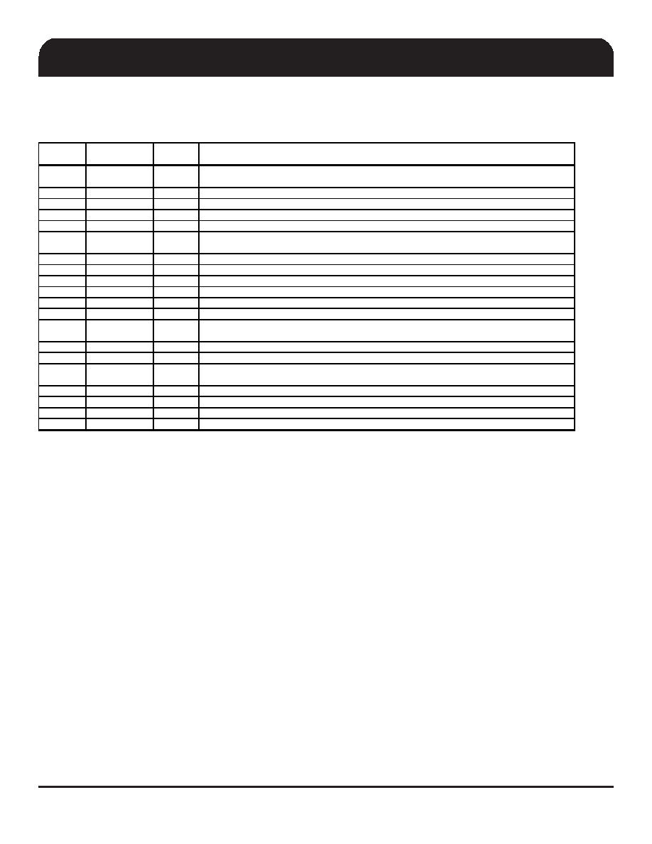
TSSOP Pin Description
PIN #
(TSSOP)
PIN NAME
PIN TYPE
DESCRIPTION
1OE0#
IN
Output Enable for DIF0 output. Control is as follows:
0 = enabled, 1 = Low-Low
2
DIF_INC
IN
Complement side of differential input clock
3
DIF_INT
IN
True side of differential input clock
4
VDDA
PWR
3.3V Power for the Analog Core
5
GNDA
GND
Ground for the Analog Core
6OE3#
IN
Output Enable for DIF3 output. Control is as follows:
0 = enabled, 1 = Low-Low
7
DIF3C_LPR
OUT
Complement clock of low power differential clock pair. (no 50ohm shunt resistor to GND needed)
8
DIF3T_LPR
OUT
True clock of low power differential clock pair. (no 50ohm shunt resistor to GND needed)
9
VDD_IO
PWR
Power supply for low power differential outputs, nominal 1.05V to 3.3V
10
GND
Ground pin
11
DIF2C_LPR
OUT
Complement clock of low power differential clock pair. (no 50ohm shunt resistor to GND needed)
12
DIF2T_LPR
OUT
True clock of low power differential clock pair. (no 50ohm shunt resistor to GND needed)
13
OE2#
IN
Output Enable for DIF2 output. Control is as follows:
0 = enabled, 1 = Low-Low
14
DIF1C_LPR
OUT
Complement clock of low power differential clock pair. (no 50ohm shunt resistor to GND needed)
15
DIF1T_LPR
OUT
True clock of low power differential clock pair. (no 50ohm shunt resistor to GND needed)
16
OE1#
IN
Output Enable for DIF1 output. Control is as follows:
0 = enabled, 1 = Low-Low
17
GND
Ground pin
18
VDD_IO
PWR
Power supply for low power differential outputs, nominal 1.05V to 3.3V
19
DIF0C_LPR
OUT
Complement clock of low power differential clock pair. (no 50ohm shunt resistor to GND needed)
20
DIF0T_LPR
OUT
True clock of low power differential clock pair. (no 50ohm shunt resistor to GND needed)
相关PDF资料 |
PDF描述 |
|---|---|
| 9DBL411AGLF | LOW SKEW CLOCK DRIVER, PDSO20 |
| 9DBL411BKILF | LOW SKEW CLOCK DRIVER, PQCC20 |
| 9DBL411BGILF | LOW SKEW CLOCK DRIVER, PDSO20 |
| 9DBL411BGILFT | LOW SKEW CLOCK DRIVER, PDSO20 |
| 9DBL411BKLF | LOW SKEW CLOCK DRIVER, PQCC20 |
相关代理商/技术参数 |
参数描述 |
|---|---|
| 9DBL411B | 制造商:IDT 制造商全称:Integrated Device Technology 功能描述:Four Output Low Power Differential Fanout Buffer for PCI Express Gen1, Gen2, and QPI |
| 9DBL411BGILF | 功能描述:时钟缓冲器 LOW POWER PCIE/QPI w /POWER DOWN FEATURE RoHS:否 制造商:Texas Instruments 输出端数量:5 最大输入频率:40 MHz 传播延迟(最大值): 电源电压-最大:3.45 V 电源电压-最小:2.375 V 最大功率耗散: 最大工作温度:+ 85 C 最小工作温度:- 40 C 封装 / 箱体:LLP-24 封装:Reel |
| 9DBL411BGILFT | 功能描述:时钟缓冲器 LOW POWER PCIE/QPI w /POWER DOWN FEATURE RoHS:否 制造商:Texas Instruments 输出端数量:5 最大输入频率:40 MHz 传播延迟(最大值): 电源电压-最大:3.45 V 电源电压-最小:2.375 V 最大功率耗散: 最大工作温度:+ 85 C 最小工作温度:- 40 C 封装 / 箱体:LLP-24 封装:Reel |
| 9DBL411BGLF | 功能描述:时钟缓冲器 LOW POWER PCIE/QPI w /POWER DOWN FEATURE RoHS:否 制造商:Texas Instruments 输出端数量:5 最大输入频率:40 MHz 传播延迟(最大值): 电源电压-最大:3.45 V 电源电压-最小:2.375 V 最大功率耗散: 最大工作温度:+ 85 C 最小工作温度:- 40 C 封装 / 箱体:LLP-24 封装:Reel |
| 9DBL411BGLFT | 功能描述:时钟缓冲器 LOW POWER PCIE/QPI w /POWER DOWN FEATURE RoHS:否 制造商:Texas Instruments 输出端数量:5 最大输入频率:40 MHz 传播延迟(最大值): 电源电压-最大:3.45 V 电源电压-最小:2.375 V 最大功率耗散: 最大工作温度:+ 85 C 最小工作温度:- 40 C 封装 / 箱体:LLP-24 封装:Reel |
发布紧急采购,3分钟左右您将得到回复。