- 您现在的位置:买卖IC网 > PDF目录25565 > 9DBL411BGLFT (INTEGRATED DEVICE TECHNOLOGY INC) LOW SKEW CLOCK DRIVER, PDSO20 PDF资料下载
参数资料
| 型号: | 9DBL411BGLFT |
| 厂商: | INTEGRATED DEVICE TECHNOLOGY INC |
| 元件分类: | 时钟及定时 |
| 英文描述: | LOW SKEW CLOCK DRIVER, PDSO20 |
| 封装: | 4.40 MM, 0.65 MM PITCH, ROHS COMPLIANT, MO-153, TSSOP-20 |
| 文件页数: | 6/9页 |
| 文件大小: | 85K |
| 代理商: | 9DBL411BGLFT |
IDT Four Output Low Power Differential Buffer for PCI Express for Gen1, Gen2, and QPI
1645B—04/23/10
Advance Information
ICS9DBL411B
Four Output Low Power Differential Buffer for PCI Express Gen1, Gen2, and QPI
6
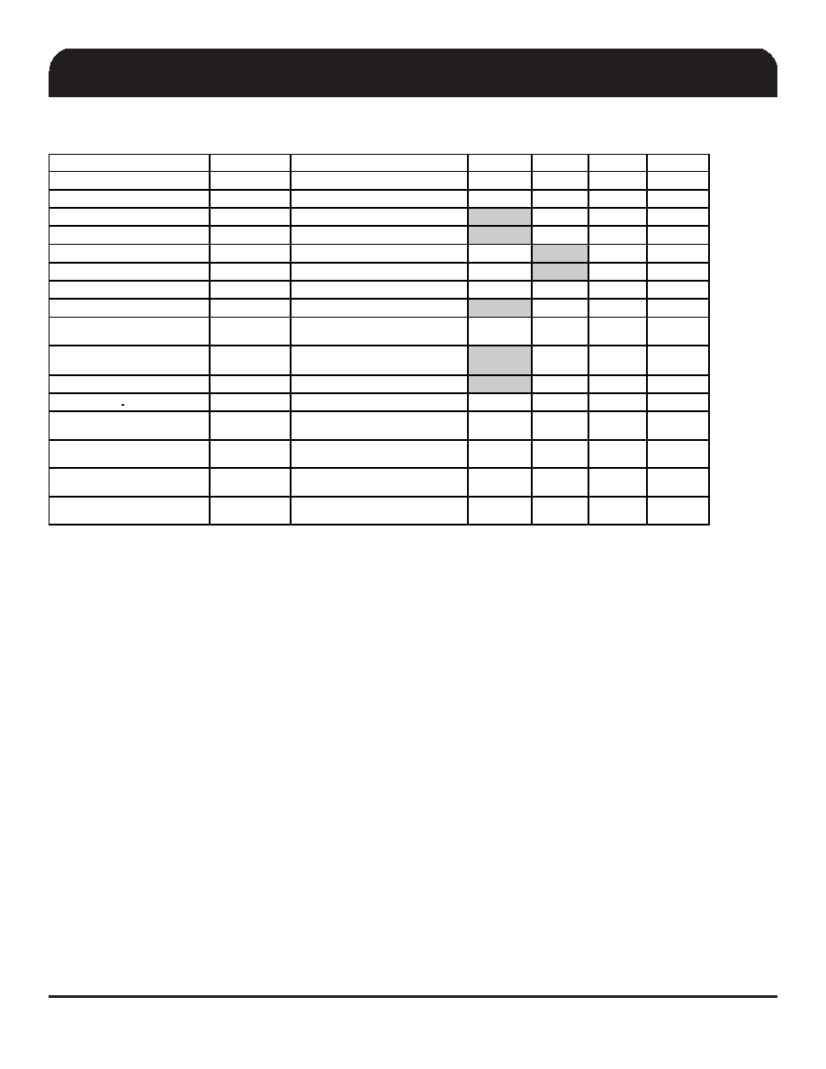
AC Electrical Characteristics - DIF Low Power Differential Outputs
PARAMETER
SYMBOL
CONDITIONS
MIN
MAX
UNITS
NOTES
Rising Edge Slew Rate
t
SLR
Differential Measurement
1.5
4
V/ns
1,2
Falling Edge Slew Rate
t
FLR
Differential Measurement
1.5
4
V/ns
1,2
Slew Rate Variation
t
SLVAR
Single-ended Measurement
20
%
1
Maximum Output Voltage
V
HIGH
Includes overshoot
1150
mV
1
Minimum Output Voltage
V
LOW
Includes undershoot
-300
mV
1
Differential Voltage Swing
V
SWING
Differential Measurement
1200
mV
1
Crossing Point Voltage
V
XABS
Single-ended Measurement
300
550
mV
1,3,4
Crossing Point Variation
V
XABSVAR
Single-ended Measurement
140
mV
1,3,5
Duty Cycle Distortion
D
CYCDIS0
Differential Measurement,
fIN<=133.33MHz
3%
1,6
Additive Cycle to Cycle Jitter
DIFJ
C2CADD
Differential Measurement,
Additive
15
ps
1
DIF[3:0] Skew
DIF
SKEW
Differential Measurement
50
ps
1
Propagation Delay
t
PD
Input to output Delay
2.5
3.5
ns
1
Additive Phase Jitter - PCIe
Gen1
t
phase_addPCIG1
1.5MHz < 22MHz
6
ps Pk-Pk
1,9
Additive Phase Jitter - PCIe
Gen2 High Band
t
phase_addPCIG2HI
High Band is 1.5MHz to Nyquist
(50MHz)
0.16
ps rms
1,9
Additive Phase Jitter PCIe
Gen2 Low Band
t
phase_addPCIG2LO
Low Band is 10KHz to 1.5MHz
0.07
ps rms
1,9
Additive Phase Jitter QPI133
(6.4GBs, 12 UI)
t
phase_addQPI6G4
11MHz to 33MHz
0.04
ps rms
1,9
Notes on Electrical Characteristics (all measurements use 9LRS3187B as clock source and RS=33ohms/CL=2pF test load):
1Guaranteed by design and characterization, not 100% tested in production.
2 Slew rate measured through Vswing centered around differential zero
3 Vxabs is defined as the voltage where CLK = CLK#
4 Only applies to the differential rising edge (CLK rising and CLK# falling)
9 The 9DBL411B has no PLL, so the part itself contributes very little jitter to the input clock. But this also means that the 9DBL411
cannot 'de-jitter' a noisy input clock. Values calculated per PCI SIG and per Intel Clock Jitter tool version 1.5
8 Maximum input voltage is not to exceed maximum VDD
6 This figure refers to the maximum distortion of the input wave form.
5 Defined as the total variation of all crossing voltages of CLK rising and CLK# falling. Matching applies to rising edge rate of CLK and
falling edge of CLK#. It is measured using a +/-75mV window centered on the average cross point where CLK meets CLK#.
7 Operation under these conditions is neither implied, nor guaranteed.
相关PDF资料 |
PDF描述 |
|---|---|
| 9DBL411BKILFT | LOW SKEW CLOCK DRIVER, PQCC20 |
| 9DBL411BGLF | LOW SKEW CLOCK DRIVER, PDSO20 |
| 9E4101YFILFT | MICROCONTROLLER, PDSO56 |
| 9EPRS475CGLF | PROC SPECIFIC CLOCK GENERATOR, PDSO56 |
| 9EPRS475CGLFT | PROC SPECIFIC CLOCK GENERATOR, PDSO56 |
相关代理商/技术参数 |
参数描述 |
|---|---|
| 9DBL411BKILF | 功能描述:时钟缓冲器 LOW POWER PCIE/QPI w /POWER DOWN FEATURE RoHS:否 制造商:Texas Instruments 输出端数量:5 最大输入频率:40 MHz 传播延迟(最大值): 电源电压-最大:3.45 V 电源电压-最小:2.375 V 最大功率耗散: 最大工作温度:+ 85 C 最小工作温度:- 40 C 封装 / 箱体:LLP-24 封装:Reel |
| 9DBL411BKILFT | 功能描述:时钟缓冲器 LOW POWER PCIE/QPI w /POWER DOWN FEATURE RoHS:否 制造商:Texas Instruments 输出端数量:5 最大输入频率:40 MHz 传播延迟(最大值): 电源电压-最大:3.45 V 电源电压-最小:2.375 V 最大功率耗散: 最大工作温度:+ 85 C 最小工作温度:- 40 C 封装 / 箱体:LLP-24 封装:Reel |
| 9DBL411BKLF | 功能描述:时钟缓冲器 LOW POWER PCIE/QPI w /POWER DOWN FEATURE RoHS:否 制造商:Texas Instruments 输出端数量:5 最大输入频率:40 MHz 传播延迟(最大值): 电源电压-最大:3.45 V 电源电压-最小:2.375 V 最大功率耗散: 最大工作温度:+ 85 C 最小工作温度:- 40 C 封装 / 箱体:LLP-24 封装:Reel |
| 9DBL411BKLFT | 功能描述:时钟缓冲器 LOW POWER PCIE/QPI w /POWER DOWN FEATURE RoHS:否 制造商:Texas Instruments 输出端数量:5 最大输入频率:40 MHz 传播延迟(最大值): 电源电压-最大:3.45 V 电源电压-最小:2.375 V 最大功率耗散: 最大工作温度:+ 85 C 最小工作温度:- 40 C 封装 / 箱体:LLP-24 封装:Reel |
| 9DBU0231AKILF | 功能描述:IC BUFFER 2OUTPUT 1.5V 24VFQFPN 制造商:idt, integrated device technology inc 系列:- 包装:管件 零件状态:有效 PLL:是 主要用途:PCI Express(PCIe) 输入:HCSL 输出:LP-HCSL 电路数:1 比率 - 输入:输出:1:2 差分 - 输入:输出:是/是 频率 - 最大值:167MHz 电压 - 电源:1.425 V ~ 1.575 V 工作温度:-40°C ~ 85°C 安装类型:表面贴装 封装/外壳:24-VFQFN 裸露焊盘 供应商器件封装:24-QFN(4x4) 标准包装:75 |
发布紧急采购,3分钟左右您将得到回复。