- 您现在的位置:买卖IC网 > PDF目录25565 > 9DBL411BKILFT (INTEGRATED DEVICE TECHNOLOGY INC) LOW SKEW CLOCK DRIVER, PQCC20 PDF资料下载
参数资料
| 型号: | 9DBL411BKILFT |
| 厂商: | INTEGRATED DEVICE TECHNOLOGY INC |
| 元件分类: | 时钟及定时 |
| 英文描述: | LOW SKEW CLOCK DRIVER, PQCC20 |
| 封装: | ROHS COMPLIANT, PLASTIC, MLF-20 |
| 文件页数: | 4/9页 |
| 文件大小: | 85K |
| 代理商: | 9DBL411BKILFT |
IDT Four Output Low Power Differential Buffer for PCI Express for Gen1, Gen2, and QPI
1645B—04/23/10
Advance Information
ICS9DBL411B
Four Output Low Power Differential Buffer for PCI Express Gen1, Gen2, and QPI
4
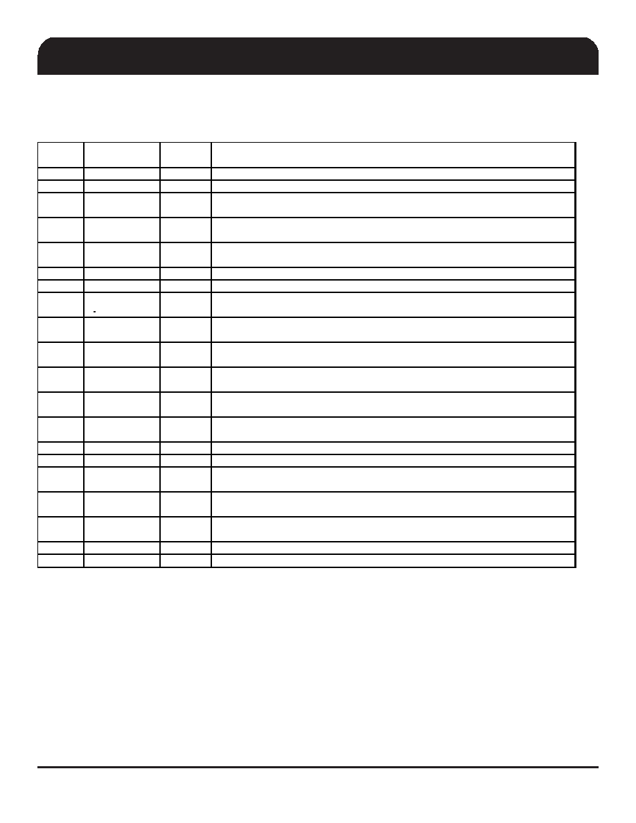
MLF Pin Description
PIN #
(MLF)
PIN NAME
PIN TYPE
DESCRIPTION
1
VDDA
PWR
3.3V Power for the Analog Core
2
GNDA
GND
Ground for the Analog Core
3OE3#
IN
Output Enable for DIF3 output. Control is as follows:
0 = enabled, 1 = Low-Low
4
DIF3C_LPR
OUT
Complement clock of low power differential clock pair. (no 50ohm shunt resistor to
GND needed)
5
DIF3T_LPR
OUT
True clock of low power differential clock pair. (no 50ohm shunt resistor to GND
needed)
6
VDD_IO
PWR
Power supply for low power differential outputs, nominal 1.05V to 3.3V
7
GND
Ground pin
8
DIF2C_LPR
OUT
Complement clock of low power differential clock pair. (no 50ohm shunt resistor to
GND needed)
9
DIF2T_LPR
OUT
True clock of low power differential clock pair. (no 50ohm shunt resistor to GND
needed)
10
OE2#
IN
Output Enable for DIF2 output. Control is as follows:
0 = enabled, 1 = Low-Low
11
DIF1C_LPR
OUT
Complement clock of low power differential clock pair. (no 50ohm shunt resistor to
GND needed)
12
DIF1T_LPR
OUT
True clock of low power differential clock pair. (no 50ohm shunt resistor to GND
needed)
13
OE1#
IN
Output Enable for DIF1 output. Control is as follows:
0 = enabled, 1 = Low-Low
14
GND
Ground pin
15
VDD_IO
PWR
Power supply for low power differential outputs, nominal 1.05V to 3.3V
16
DIF0C_LPR
OUT
Complement clock of low power differential clock pair. (no 50ohm shunt resistor to
GND needed)
17
DIF0T_LPR
OUT
True clock of low power differential clock pair. (no 50ohm shunt resistor to GND
needed)
18
OE0#
IN
Output Enable for DIF0 output. Control is as follows:
0 = enabled, 1 = Low-Low
19
DIF_INC
IN
Complement side of differential input clock
20
DIF_INT
IN
True side of differential input clock
相关PDF资料 |
PDF描述 |
|---|---|
| 9DBL411BGLF | LOW SKEW CLOCK DRIVER, PDSO20 |
| 9E4101YFILFT | MICROCONTROLLER, PDSO56 |
| 9EPRS475CGLF | PROC SPECIFIC CLOCK GENERATOR, PDSO56 |
| 9EPRS475CGLFT | PROC SPECIFIC CLOCK GENERATOR, PDSO56 |
| 9EPRS488CKLF | SPECIALTY MICROPROCESSOR CIRCUIT, PQCC72 |
相关代理商/技术参数 |
参数描述 |
|---|---|
| 9DBL411BKLF | 功能描述:时钟缓冲器 LOW POWER PCIE/QPI w /POWER DOWN FEATURE RoHS:否 制造商:Texas Instruments 输出端数量:5 最大输入频率:40 MHz 传播延迟(最大值): 电源电压-最大:3.45 V 电源电压-最小:2.375 V 最大功率耗散: 最大工作温度:+ 85 C 最小工作温度:- 40 C 封装 / 箱体:LLP-24 封装:Reel |
| 9DBL411BKLFT | 功能描述:时钟缓冲器 LOW POWER PCIE/QPI w /POWER DOWN FEATURE RoHS:否 制造商:Texas Instruments 输出端数量:5 最大输入频率:40 MHz 传播延迟(最大值): 电源电压-最大:3.45 V 电源电压-最小:2.375 V 最大功率耗散: 最大工作温度:+ 85 C 最小工作温度:- 40 C 封装 / 箱体:LLP-24 封装:Reel |
| 9DBU0231AKILF | 功能描述:IC BUFFER 2OUTPUT 1.5V 24VFQFPN 制造商:idt, integrated device technology inc 系列:- 包装:管件 零件状态:有效 PLL:是 主要用途:PCI Express(PCIe) 输入:HCSL 输出:LP-HCSL 电路数:1 比率 - 输入:输出:1:2 差分 - 输入:输出:是/是 频率 - 最大值:167MHz 电压 - 电源:1.425 V ~ 1.575 V 工作温度:-40°C ~ 85°C 安装类型:表面贴装 封装/外壳:24-VFQFN 裸露焊盘 供应商器件封装:24-QFN(4x4) 标准包装:75 |
| 9DBU0231AKLF | 功能描述:IC BUFFER 2OUTPUT 1.5V 24VFQFPN 制造商:idt, integrated device technology inc 系列:- 包装:管件 零件状态:有效 PLL:是 主要用途:PCI Express(PCIe) 输入:HCSL 输出:LP-HCSL 电路数:1 比率 - 输入:输出:1:2 差分 - 输入:输出:是/是 频率 - 最大值:167MHz 电压 - 电源:1.425 V ~ 1.575 V 工作温度:0°C ~ 70°C 安装类型:表面贴装 封装/外壳:24-VFQFN 裸露焊盘 供应商器件封装:24-QFN(4x4) 标准包装:75 |
| 9DBU0241AKILF | 功能描述:IC BUFFER 2OUTPUT 1.5V 24MLF 制造商:idt, integrated device technology inc 系列:- 包装:管件 零件状态:有效 PLL:是 主要用途:PCI Express(PCIe) 输入:HCSL 输出:LP-HCSL 电路数:1 比率 - 输入:输出:1:2 差分 - 输入:输出:是/是 频率 - 最大值:167MHz 电压 - 电源:1.425 V ~ 1.575 V 工作温度:-40°C ~ 85°C 安装类型:表面贴装 封装/外壳:24-VFQFN 裸露焊盘 供应商器件封装:24-QFN(4x4) 标准包装:75 |
发布紧急采购,3分钟左右您将得到回复。