- 您现在的位置:买卖IC网 > PDF目录122717 > 9ERS3165BGILF (INTEGRATED DEVICE TECHNOLOGY INC) 400 MHz, PROC SPECIFIC CLOCK GENERATOR, PDSO64 PDF资料下载
参数资料
| 型号: | 9ERS3165BGILF |
| 厂商: | INTEGRATED DEVICE TECHNOLOGY INC |
| 元件分类: | 时钟产生/分配 |
| 英文描述: | 400 MHz, PROC SPECIFIC CLOCK GENERATOR, PDSO64 |
| 封装: | 6.10 MM, 0.50 MM PITCH, ROHS COMPLIANT, TSSOP-64 |
| 文件页数: | 13/26页 |
| 文件大小: | 319K |
| 代理商: | 9ERS3165BGILF |
IDTTM
Embedded 64-Pin Industrial Temperature Range CK505 Compatible Clock
1613B—01/25/10
ICS9ERS3165
Embedded 64-Pin Industrial Temperature Range CK505 Compatible Clock
20
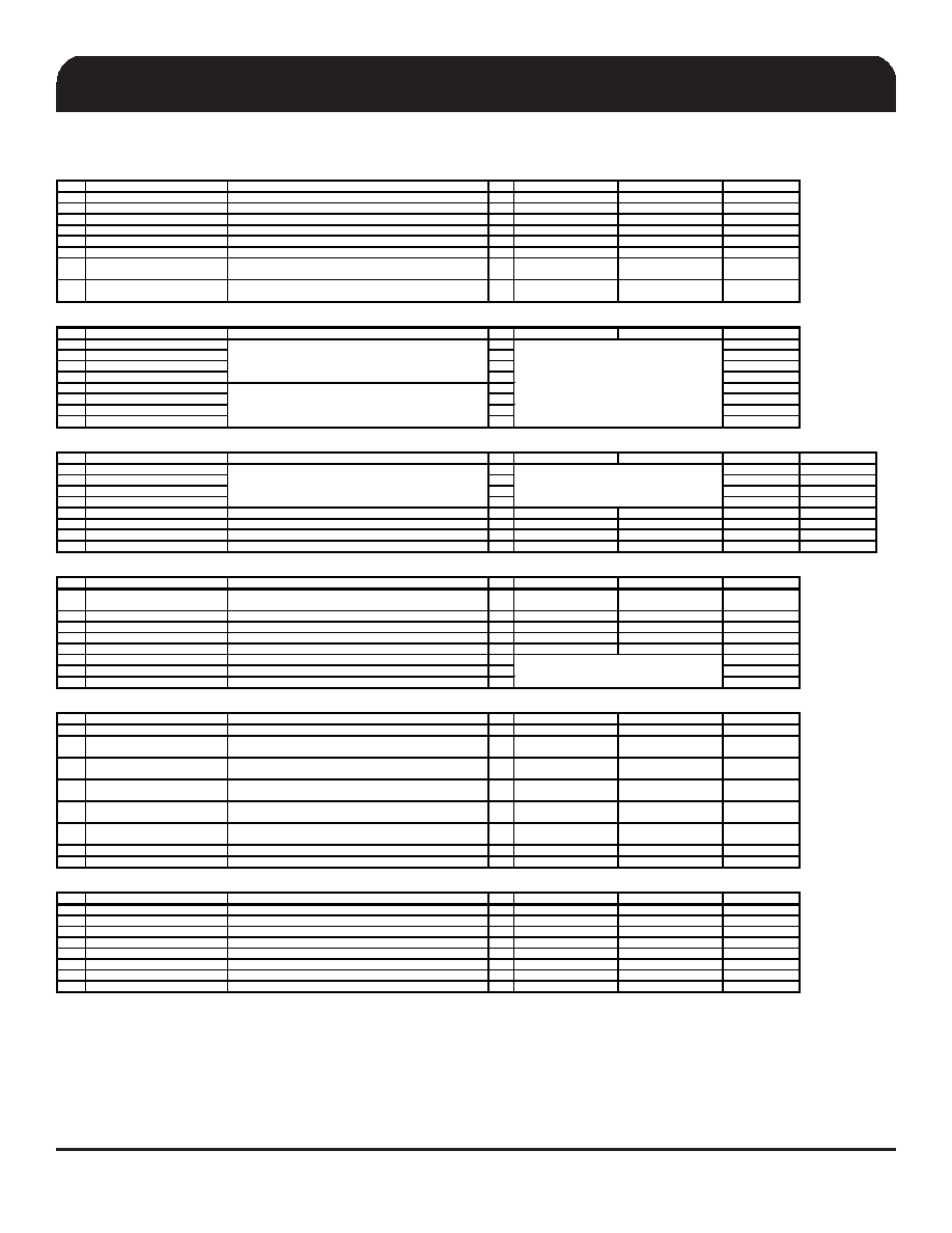
Byte 6 Clock Request Enable/Configuration Register
Bit
Name
Description
Type
0
1
Default
7
CR#_E_EN
Enable CR#_E (clk req) for SRC6
RW
Disable CR#_E
Enable CR#_E
0
6
CR#_F_EN
Enable CR#_F (clk req) for SRC8
RW
Disable CR#_F
Enable CR#_F
0
5
CR#_G_EN
Enable CR#_G (clk req) for SRC9
RW
Disable CR#_G
Enable CR#_G
0
4
CR#_H_EN
Enable CR#_H (clk req) for SRC10
RW
Disable CR#_H
Enable CR#_H
0
3
Reserved
RW
-
0
2
Reserved
RW
-
0
1
LCD/SRC1_STP_CRTL
If set, LCD_SS/SRC1 stops with PCI_STOP#
RW
Free Running
Stops with PCI_STOP#
assertion
0
SRC0_STP_CRTL
If set, SRC0 stop with PCI_STOP#
RW
Free Running
Stops with PCI_STOP#
assertion
0
Byte 7 Vendor ID/ Revision ID Register
Bit
Name
Description
Type
0
1
Default
7
Rev Code Bit 3
R0
6
Rev Code Bit 2
R0
5
Rev Code Bit 1
R0
4
Rev Code Bit 0
R1
3
Vendor ID bit 3
R0
2
Vendor ID bit 2
R0
1
Vendor ID bit 1
R0
0
Vendor ID bit 0
R1
Byte 8 Device ID & Output Enable Register
Bit
Name
Description
Type
0
1
Default (TSSOP)
Default (MLF)
7
Device_ID3
R0
0
6
Device_ID2
R0
0
5
Device_ID1
R0
0
4
Device_ID0
R1
0
3
Reserved
RW
--
00
2
Reserved
RW
-
0
1
27MHz_nonSS/SE1_OE
Output enable for SE1
RW
Disabled
Enabled
1
0
27MHz_SS/SE2_OE
Output enable for SE2
RW
Disabled
Enabled
11
Byte 9 Test and Output Control Register
Bit
Name
Description
Type
0
1
Default
7
PCIF5 STOP EN
Allows control of PCIF5 with assertion of PCI_STOP#
RW
Free running
Stops with PCI_STOP#
assertion
0
6
TME_Readback
Truested Mode Enable (TME) strap status
R
normal operation
no overclocking
TME latch
5
Reserved
RW
--
1
4
Test Mode Select
Allows test select, ignores REF/FSC/TestSel
RW
Outputs HI-Z
Outputs = REF/N
0
3
Test Mode Entry
Allows entry into test mode, ignores FSB/TestMode
RW
Normal operation
Test mode
0
2
CPU IO_VOUT2
CPU IO Output Voltage Select (Most Significant Bit)
RW
1
CPU IO_VOUT1
CPU IO Output Voltage Select
RW
0
CPU IO_VOUT0
CPU IO Output Voltage Select (Least Significant Bit)
RW
1
Byte 10 Output Control Register
Bit
Name
Description
Type
0
1
Default
7
27_SEL Latch Readback
Readback of 27_Select latch
R
Dot96/ LCD_SS /SE
SRC0/ 27MHz
27_SEL latch
6
PCI4 STOP EN
Allows control of PCI4 with assertion of PCI_STOP#
RW
Free running
Stops with PCI_STOP#
assertion
1
5
PCI3 STOP EN
Allows control of PCI3 with assertion of PCI_STOP#
RW
Free running
Stops with PCI_STOP#
assertion
1
4
PCI2 STOP EN
Allows control of PCI2 with assertion of PCI_STOP#
RW
Free running
Stops with PCI_STOP#
assertion
1
3
PCI1 STOP EN
Allows control of PCI1 with assertion of PCI_STOP#
RW
Free running
Stops with PCI_STOP#
assertion
1
2
PCI0 STOP EN
Allows control of PCI0 with assertion of PCI_STOP#
RW
Free running
Stops with PCI_STOP#
assertion
1
CPU1 Stop Enable
Enables control of CPU1 with CPU_STOP#
RW
Free Running
Stoppable
1
0
CPU0 Stop Enable
Enables control of CPU0 with CPU_STOP#
RW
Free Running
Stoppable
1
Byte 11 iAMT/CPU2 Control Register
Bit
Name
Description
Type
0
1
Default
7
Reserved
RW
--
0
6
Reserved
RW
-
0
5
Reserved
RW
-
0
4
Reserved
RW
--
0
3
CPU2_AMT_EN
M1 mode clk enable, only if ITP_EN=1
RW
Disable
Enable
0
2
CPU1_AMT_EN
M1 mode clk enable
RW
Disable
Enable
1
Reserved
RW
--
0
CPU2 Stop Enable
Enables control of CPU2 with CPU_STOP#
RW
Free Running
Stoppable
1
Revision ID
Vendor specific
Vendor ID
ICS is 0001, binary
Table of Device identifier codes, used for differentiating between
CK505 package options, etc.
See Device ID Table 4
See Table 3: V_IO Selection
(Default is 0.8V)
相关PDF资料 |
PDF描述 |
|---|---|
| 9LPRS535BFLFT | SPECIALTY MICROPROCESSOR CIRCUIT, PDSO48 |
| 935208500112 | 8-BIT, 16 MHz, MICROCONTROLLER, PDIP40 |
| 935208540112 | 8-BIT, 16 MHz, MICROCONTROLLER, PQCC44 |
| 935267591518 | 8-BIT, MROM, 16 MHz, MICROCONTROLLER, PQFP44 |
| 935262073551 | 8-BIT, MROM, 25 MHz, MICROCONTROLLER, PQFP64 |
相关代理商/技术参数 |
参数描述 |
|---|---|
| 9ERS3165BGILFT | 功能描述:时钟合成器/抖动清除器 EMBEDDED CK505 COMPATIBLE CLOCK RoHS:否 制造商:Skyworks Solutions, Inc. 输出端数量: 输出电平: 最大输出频率: 输入电平: 最大输入频率:6.1 GHz 电源电压-最大:3.3 V 电源电压-最小:2.7 V 封装 / 箱体:TSSOP-28 封装:Reel |
| 9ERS3165BGLF | 功能描述:时钟合成器/抖动清除器 EMBEDDED CK505 COMPATIBLE CLOCK RoHS:否 制造商:Skyworks Solutions, Inc. 输出端数量: 输出电平: 最大输出频率: 输入电平: 最大输入频率:6.1 GHz 电源电压-最大:3.3 V 电源电压-最小:2.7 V 封装 / 箱体:TSSOP-28 封装:Reel |
| 9ERS3165BGLFT | 功能描述:时钟合成器/抖动清除器 EMBEDDED CK505 COMPATIBLE CLOCK RoHS:否 制造商:Skyworks Solutions, Inc. 输出端数量: 输出电平: 最大输出频率: 输入电平: 最大输入频率:6.1 GHz 电源电压-最大:3.3 V 电源电压-最小:2.7 V 封装 / 箱体:TSSOP-28 封装:Reel |
| 9ERS3165BKILF | 功能描述:时钟合成器/抖动清除器 EMBEDDED CK505 COMPATIBLE CLOCK RoHS:否 制造商:Skyworks Solutions, Inc. 输出端数量: 输出电平: 最大输出频率: 输入电平: 最大输入频率:6.1 GHz 电源电压-最大:3.3 V 电源电压-最小:2.7 V 封装 / 箱体:TSSOP-28 封装:Reel |
| 9ERS3165BKILFT | 功能描述:时钟合成器/抖动清除器 EMBEDDED CK505 COMPATIBLE CLOCK RoHS:否 制造商:Skyworks Solutions, Inc. 输出端数量: 输出电平: 最大输出频率: 输入电平: 最大输入频率:6.1 GHz 电源电压-最大:3.3 V 电源电压-最小:2.7 V 封装 / 箱体:TSSOP-28 封装:Reel |
发布紧急采购,3分钟左右您将得到回复。