- 您现在的位置:买卖IC网 > Datasheet目录59 > A1356LKB-T (Allegro Microsystems Inc)IC SENSOR HALL EFFECT 3 SIP Datasheet资料下载
参数资料
| 型号: | A1356LKB-T |
| 厂商: | Allegro Microsystems Inc |
| 文件页数: | 8/20页 |
| 文件大小: | 432K |
| 描述: | IC SENSOR HALL EFFECT 3 SIP |
| 标准包装: | 4,000 |
| 传感范围: | 45m%D/G ~ 75m%D/G |
| 类型: | 线性 - 可编程 |
| 电源电压: | 4.5 V ~ 18 V |
| 电流 - 电源: | 10mA |
| 电流 - 输出(最大): | 25mA |
| 输出类型: | 数字式, PWM 编码 |
| 特点: | 高精度 |
| 工作温度: | -40°C ~ 150°C |
| 封装/外壳: | 3-SIP |
| 供应商设备封装: | 3-SIP |
| 包装: | 散装 |
| 其它名称: | 620-1369 A1356LK-T |
High Precision Linear Hall-Effect Sensor IC
With an Open Drain Pulse Width Modulated Output
A1356
8
Allegro MicroSystems, LLC
115 Northeast Cutoff
Worcester, Massachusetts 01615-0036 U.S.A.
1.508.853.5000; www.allegromicro.com
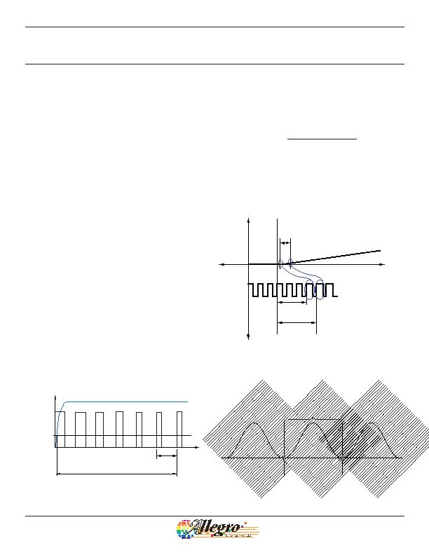
Characteristic Definitions
Power-On Time When the supply is ramped to its operating
voltage, the device requires a finite time to power its internal
components before supplying a valid PWM output duty-cycle.
Power-On Time, t
PO
, is defined as the time it takes for the output
voltage to settle within ?0% of its steady state value after the
power supply has reached its minimum specified operating volt-
age, V
CC
(min). (See figure 1.)
Propagation Delay Traveling time of signal from input Hall
plate to output stage of device. (See figure 2.)
Response Time The time interval between a) when the applied
magnetic field reaches 90% of its final value, and b) when the
sensor IC reaches 90% of its output corresponding to the applied
magnetic field. (See figure 2.)
PWM Rise Time The time elapsed between 10% and 90% of
the rising signal value when output switches from low to high
states.
PWM Fall Time The time elapsed between 90% and 10% of the
falling signal value when output switches from high to low states.
Quiescent Duty Cycle In the quiescent state (no significant
magnetic field: B = 0 G), the output duty cycle, D
(Q)
, equals a
specific programmed duty cycle throughout the entire operating
ranges of V
CC
and ambient temperature, T
A
.
Guaranteed Quiescent Duty Cycle Output Range The
Quiescent Duty Cycle Output, D
(Q)
, can be programmed around
its nominal value of 50% D, within the Guaranteed Quiescent
Duty Cycle Range limits: D
(Q)
(min) and D
(Q)
(max). The available
guaranteed programming range for D
(Q)
falls within the distribu-
tions of the minimum and the maximum programming code for
setting D
(Q)
. (See figure 3.)
Average Quiescent Duty Cycle Output Step Size The
average quiescent duty cycle output step size for a single device
is determined using the following calculation:
D
(Q)
(max)
D
(Q)
(min)
2
n
1
Step
D(Q)
=
,
(1)
where:
n is the number of available programming bits in the trim range,
2
n
1 is the value of programming steps in the range,
D
(Q)
(max) is the maximum reached quiescent duty cycle, and
D
(Q)
(min) is minimum reached quiescent duty cycle.
Figure 1. Definition of Power-On Time
Figure 2. Definitions of Propagation Delay and Response Time
Figure 3. Definition of Guaranteed Quiescent Voltage Output Range
Guaranteed D
(Q)
Programming
Range
D
(Q)
(min)
D
(Q)
(max)
Max Code D
(Q)
Distribution
Min Code D
(Q)
Distribution
Initial D
(Q)
Distribution
Propagation
Delay
0.5 ms
Output
Time
Applied Magnetic
Field, B
Response
Time
Time
V+
V
CC
(min)
t
PO
First valid duty cycle
V
CC
A1356
Output
相关PDF资料 |
PDF描述 |
|---|---|
| A1361LKTTN-T | IC HALL EFFECT SENSOR LN 4-SIP |
| A1374EKB-T | IC SENSOR HALL EFFECT PREC 3-SIP |
| A1422LK | IC SENSOR HALL EFFECT AC 4-SIP |
| A1425LK | IC SENSOR HALL EFFECT AC 4-SIP |
| A1645LK-I2 | IC SENSOR HALL EFFECT AC 4-SIP |
相关代理商/技术参数 |
参数描述 |
|---|---|
| A1357 | 制造商:ALLEGRO 制造商全称:Allegro MicroSystems 功能描述:Two-Wire High Precision Linear Hall-Effect Sensor IC |
| A1357LKB-T | 功能描述:IC HALL EFFECT SWITCH 3-SIP RoHS:是 类别:传感器,转换器 >> 磁性 - 霍尔效应,数字式开关,线性,罗盘 (IC) 系列:- 标准包装:1 系列:- 传感范围:20mT ~ 80mT 类型:旋转 电源电压:4.5 V ~ 5.5 V 电流 - 电源:15mA 电流 - 输出(最大):- 输出类型:数字式,PWM,8.5 位串行 特点:可编程 工作温度:-40°C ~ 150°C 封装/外壳:20-SSOP(0.209",5.30mm 宽) 供应商设备封装:20-SSOP 包装:Digi-Reel® 其它名称:AS5132-HSST-500DKR |
| A1358 | 制造商:TOSHIBA 制造商全称:Toshiba Semiconductor 功能描述:TRANSISTOR (AUDIO FREQUENCY POWER AMPLIFIER APPLICATIONS) |
| A-1358 | 功能描述:通用继电器 DC SOLENOID. RoHS:否 制造商:Omron Electronics 触点形式:1 Form A (SPST-NO) 触点电流额定值:150 A 线圈电压:24 VDC 线圈电阻:144 Ohms 线圈电流:167 mA 切换电压:400 V 安装风格:Chassis 触点材料: |
| A13580-000 | 制造商:TE Connectivity 功能描述:Cable Markers Yellow Pack 制造商:TE Connectivity 功能描述:HTCM-SCE-TP-1/4-4H-4 - Bulk |
发布紧急采购,3分钟左右您将得到回复。