- 您现在的位置:买卖IC网 > PDF目录294783 > A1415A-2PLG84C FPGA, 200 CLBS, 1500 GATES, 200 MHz, PQCC84 PDF资料下载
参数资料
| 型号: | A1415A-2PLG84C |
| 元件分类: | FPGA |
| 英文描述: | FPGA, 200 CLBS, 1500 GATES, 200 MHz, PQCC84 |
| 封装: | PLASTIC, MS-007-AE, LCC-84 |
| 文件页数: | 6/68页 |
| 文件大小: | 489K |
| 代理商: | A1415A-2PLG84C |
第1页第2页第3页第4页第5页当前第6页第7页第8页第9页第10页第11页第12页第13页第14页第15页第16页第17页第18页第19页第20页第21页第22页第23页第24页第25页第26页第27页第28页第29页第30页第31页第32页第33页第34页第35页第36页第37页第38页第39页第40页第41页第42页第43页第44页第45页第46页第47页第48页第49页第50页第51页第52页第53页第54页第55页第56页第57页第58页第59页第60页第61页第62页第63页第64页第65页第66页第67页第68页
1-188
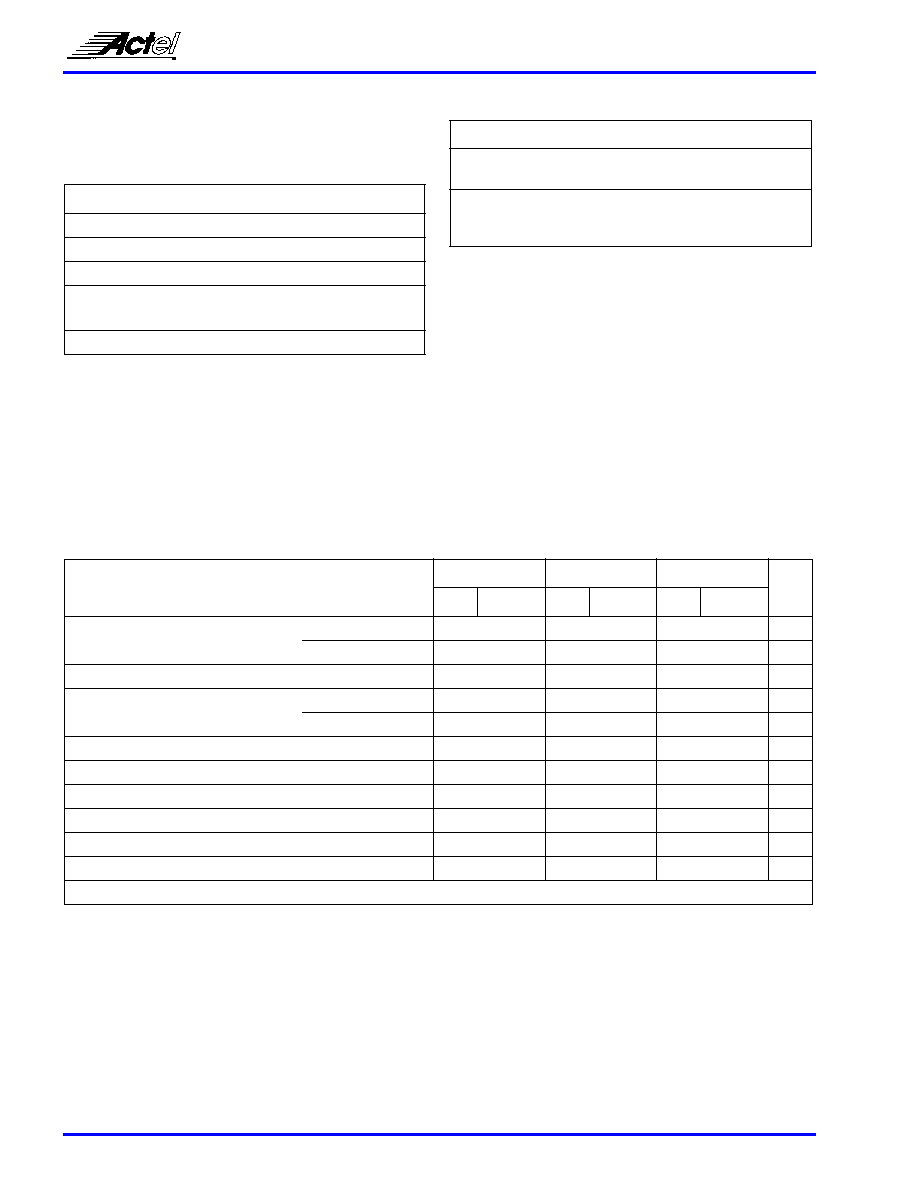
5V Operating Conditions
Absolute Maximum Ratings 1
Free air temperature range
Recommended Operating Conditions
Electrical Specifications
Symbol
Parameter
Limits
Units
VCC
DC Supply Voltage
–0.5 to +7.0
V
VI
Input Voltage
–0.5 to VCC +0.5
V
VO
Output Voltage
–0.5 to VCC +0.5
V
IIO
I/O Source Sink
Current2
±20
mA
TSTG
Storage Temperature
–65 to +150
°C
Notes:
1.
Stresses beyond those listed under “Absolute Maximum Ratings”
may cause permanent damage to the device. Exposure to
absolute maximum rated conditions for extended periods may
affect device reliability. Device should not be operated outside
the Recommended Operating Conditions.
2.
Device inputs are normally high impedance and draw
extremely low current. However, when input voltage is greater
than VCC + 0.5 V or less than GND – 0.5 V, the internal protection
diodes will forward bias and can draw excessive current.
Parameter
Commercial Industrial Military
Units
Temperature
Range1
0 to +70
–40 to +85
–55 to
+125
°C
5V Power
Supply
Tolerance
±5
±10
%VCC
Note:
1.
Ambient temperature (TA) is used for commercial and
industrial; case temperature (TC) is used for military.
Symbol Parameter
Test Condition
Commercial
Industrial
Military
Units
Min.
Max.
Min.
Max.
Min.
Max.
VOH
1,2
HIGH Level Output
IOH = –4 mA (CMOS)
3.7
V
IOH = –6 mA (CMOS) 3.84
V
IOH = –10 mA (TTL)
3
2.40
V
VOL
1,2
LOW Level Output
IOL = +6 mA (CMOS)
0.33
0.4
V
IOL = +12 mA (TTL)
3
0.50
V
VIH
HIGH Level Input
TTL Inputs
2.0
VCC + 0.3
2.0
VCC + 0.3
2.0
VCC + 0.3
V
VIL
LOW Level Input
TTL Inputs
–0.3
0.8
–0.3
0.8
–0.3
0.8
V
IIN
Input Leakage
VI = VCC or GND
–10
+10
–10
+10
–10
+10
A
IOZ
3-state Output Leakage
VO = VCC or GND
–10
+10
–10
+10
–10
+10
A
CIO
I/O Capacitance3,4
10
pF
ICC(S)
Standby VCC Supply Current (typical = 0.7 mA)
2
10
20
mA
ICC(D)
Dynamic VCC Supply Current See “Power Dissipation” Section
Notes:
1.
Actel devices can drive and receive either CMOS or TTL signal levels. No assignment of I/Os as TTL or CMOS is required.
2.
Tested one output at a time, VCC = min.
3.
Not tested, for information only.
4.
VOUT = 0V, f = 1 MHz.
5.
Typical standby current = 0.7 mA. All outputs unloaded. All inputs = VCC or GND.
相关PDF资料 |
PDF描述 |
|---|---|
| A1415A-2PLG84I | FPGA, 200 CLBS, 1500 GATES, PQCC84 |
| A1415A-2PQ100C | FPGA, 200 CLBS, 1500 GATES, 200 MHz, PQFP100 |
| A1415A-2PQ100I | FPGA, 200 CLBS, 1500 GATES, PQFP100 |
| A1415A-2PQG100C | FPGA, 200 CLBS, 1500 GATES, 200 MHz, PQFP100 |
| A1415A-2PQG100I | FPGA, 200 CLBS, 1500 GATES, PQFP100 |
相关代理商/技术参数 |
参数描述 |
|---|---|
| A1415A-2PLG84I | 制造商:Microsemi Corporation 功能描述:FPGA ACT 3 1.5K GATES 200 CELLS 200MHZ 0.8UM 5V 84PLCC - Rail/Tube |
| A1415A-2PQ100C | 制造商:Microsemi Corporation 功能描述:FPGA ACT 3 1.5K GATES 200 CELLS 200MHZ 0.8UM 5V 100PQFP - Trays 制造商:Microsemi SOC Products Group 功能描述:FPGA ACT 3 1.5K GATES 200 CELLS 200MHZ 0.8UM 5V 100PQFP - Trays |
| A1415A-2PQ100I | 制造商:Microsemi Corporation 功能描述:FPGA ACT 3 1.5K GATES 200 CELLS 200MHZ 0.8UM 5V 100PQFP - Trays |
| A1415A-2PQG100C | 制造商:Microsemi Corporation 功能描述:FPGA ACT 3 1.5K GATES 200 CELLS 200MHZ 0.8UM 5V 100PQFP - Trays |
| A1415A-2PQG100I | 制造商:Microsemi Corporation 功能描述:FPGA ACT 3 1.5K GATES 200 CELLS 200MHZ 0.8UM 5V 100PQFP - Trays |
发布紧急采购,3分钟左右您将得到回复。