- 您现在的位置:买卖IC网 > PDF目录294784 > A1415A-PL84C FPGA, 200 CLBS, 1500 GATES, 125 MHz, PQCC84 PDF资料下载
参数资料
| 型号: | A1415A-PL84C |
| 元件分类: | FPGA |
| 英文描述: | FPGA, 200 CLBS, 1500 GATES, 125 MHz, PQCC84 |
| 封装: | PLASTIC, MS-007-AE, LCC-84 |
| 文件页数: | 24/68页 |
| 文件大小: | 489K |
| 代理商: | A1415A-PL84C |
第1页第2页第3页第4页第5页第6页第7页第8页第9页第10页第11页第12页第13页第14页第15页第16页第17页第18页第19页第20页第21页第22页第23页当前第24页第25页第26页第27页第28页第29页第30页第31页第32页第33页第34页第35页第36页第37页第38页第39页第40页第41页第42页第43页第44页第45页第46页第47页第48页第49页第50页第51页第52页第53页第54页第55页第56页第57页第58页第59页第60页第61页第62页第63页第64页第65页第66页第67页第68页
1-204
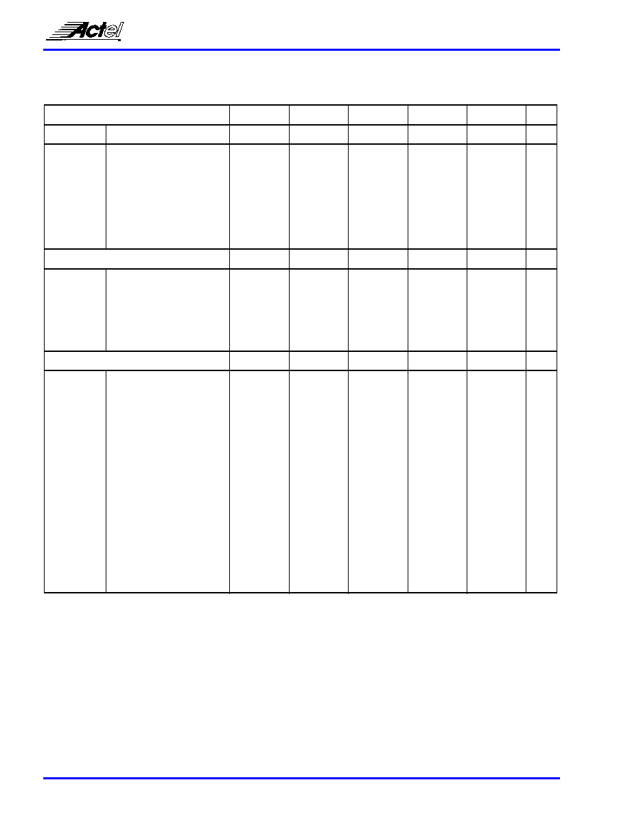
A1425A, A14V25A Timing Characteristics (continued)
(Worst-Case Commercial Conditions)
Note:
1.
Routing delays are for typical designs across worst-case operating conditions. These parameters should be used for estimating device
performance. Post-route timing analysis or simulation is required to determine actual worst-case performance. Post-route timing is based
on actual routing delay measurements performed on the device prior to shipment.
I/O Module Input Propagation Delays
‘–3’ Speed
‘–2’ Speed
‘–1’ Speed
‘Std’ Speed
3.3V Speed
Parameter
Description
Min.
Max.
Min.
Max.
Min.
Max.
Min.
Max.
Min.
Max. Units
tINY
Input Data Pad to Y
2.8
3.2
3.6
4.2
5.5
ns
tICKY
Input Reg IOCLK Pad to Y
4.7
5.3
6.0
7.0
9.2
ns
tOCKY
Output Reg IOCLK Pad to Y
4.7
5.3
6.0
7.0
9.2
ns
tICLRY
Input Asynchronous
Clear to Y
4.7
5.3
6.0
7.0
9.2
ns
tOCLRY
Output Asynchronous
Clear to Y
4.7
5.3
6.0
7.0
9.2
ns
Predicted Input Routing Delays1
tIRD1
FO=1 Routing Delay
0.9
1.0
1.1
1.3
1.7
ns
tIRD2
FO=2 Routing Delay
1.2
1.4
1.6
1.8
2.4
ns
tIRD3
FO=3 Routing Delay
1.4
1.6
1.8
2.1
2.8
ns
tIRD4
FO=4 Routing Delay
1.7
1.9
2.2
2.5
3.3
ns
tIRD8
FO=8 Routing Delay
2.8
3.2
3.6
4.2
5.5
ns
I/O Module Sequential Timing
tINH
Input F-F Data Hold
(w.r.t. IOCLK Pad)
0.0
ns
tINSU
Input F-F Data Setup
(w.r.t. IOCLK Pad)
1.8
2.0
2.3
2.7
3.0
ns
tIDEH
Input Data Enable Hold
(w.r.t. IOCLK Pad)
0.0
ns
tIDESU
Input Data Enable Setup
(w.r.t. IOCLK Pad)
5.8
6.5
7.5
8.6
ns
tOUTH
Output F-F Data Hold
(w.r.t. IOCLK Pad)
0.7
0.8
0.9
1.0
ns
tOUTSU
Output F-F Data Setup
(w.r.t. IOCLK Pad)
0.7
0.8
0.9
1.0
ns
tODEH
Output Data Enable Hold
(w.r.t. IOCLK Pad)
0.3
0.4
0.5
ns
tODESU
Output Data Enable Setup
(w.r.t. IOCLK Pad)
1.3
1.5
1.7
2.0
ns
相关PDF资料 |
PDF描述 |
|---|---|
| A1415A-PLG84C | FPGA, 200 CLBS, 1500 GATES, 125 MHz, PQCC84 |
| A1415A-PQ100C | FPGA, 200 CLBS, 1500 GATES, 125 MHz, PQFP100 |
| A1415A-PQG100C | FPGA, 200 CLBS, 1500 GATES, 125 MHz, PQFP100 |
| A1415A-VQ100C | FPGA, 200 CLBS, 1500 GATES, 125 MHz, PQFP100 |
| A1415A-VQG100C | FPGA, 200 CLBS, 1500 GATES, 125 MHz, PQFP100 |
相关代理商/技术参数 |
参数描述 |
|---|---|
| A1415A-PL84I | 功能描述:IC FPGA 1500 GATES 84-PLCC RoHS:否 类别:集成电路 (IC) >> 嵌入式 - FPGA(现场可编程门阵列) 系列:ACT™ 3 标准包装:40 系列:SX-A LAB/CLB数:6036 逻辑元件/单元数:- RAM 位总计:- 输入/输出数:360 门数:108000 电源电压:2.25 V ~ 5.25 V 安装类型:表面贴装 工作温度:0°C ~ 70°C 封装/外壳:484-BGA 供应商设备封装:484-FPBGA(27X27) |
| A1415A-PL84M | 制造商:Microsemi Corporation 功能描述:FPGA ACT 3 Family 1.5K Gates 200 Cells 125MHz 0.8um Technology 5V 84-Pin PLCC 制造商:Microsemi SOC Products Group 功能描述:FPGA ACT 3 1.5K GATES 200 CELLS 125MHZ 0.8UM 5V 84PLCC - Rail/Tube 制造商:Microsemi Corporation 功能描述:IC FPGA 1500 GATES 84-PLCC MIL |
| A1415A-PLG84C | 功能描述:IC FPGA 1500 GATES 84-PLCC RoHS:是 类别:集成电路 (IC) >> 嵌入式 - FPGA(现场可编程门阵列) 系列:ACT™ 3 标准包装:40 系列:SX-A LAB/CLB数:6036 逻辑元件/单元数:- RAM 位总计:- 输入/输出数:360 门数:108000 电源电压:2.25 V ~ 5.25 V 安装类型:表面贴装 工作温度:0°C ~ 70°C 封装/外壳:484-BGA 供应商设备封装:484-FPBGA(27X27) |
| A1415A-PLG84I | 功能描述:IC FPGA 1500 GATES 84-PLCC RoHS:是 类别:集成电路 (IC) >> 嵌入式 - FPGA(现场可编程门阵列) 系列:ACT™ 3 标准包装:40 系列:SX-A LAB/CLB数:6036 逻辑元件/单元数:- RAM 位总计:- 输入/输出数:360 门数:108000 电源电压:2.25 V ~ 5.25 V 安装类型:表面贴装 工作温度:0°C ~ 70°C 封装/外壳:484-BGA 供应商设备封装:484-FPBGA(27X27) |
| A1415A-PLG84M | 制造商:Microsemi Corporation 功能描述:FPGA ACT 3 Family 1.5K Gates 200 Cells 125MHz 0.8um (CMOS) Technology 5V 84-Pin PLCC 制造商:Microsemi SOC Products Group 功能描述:FPGA ACT 3 1.5K GATES 200 CELLS 125MHZ 0.8UM 5V 84PLCC - Rail/Tube 制造商:Microsemi Corporation 功能描述:IC FPGA 1500 GATES 84-PLCC MIL |
发布紧急采购,3分钟左右您将得到回复。