- 您现在的位置:买卖IC网 > Datasheet目录59 > A1422LK (Allegro Microsystems Inc)IC SENSOR HALL EFFECT AC 4-SIP Datasheet资料下载
参数资料
| 型号: | A1422LK |
| 厂商: | Allegro Microsystems Inc |
| 文件页数: | 5/15页 |
| 文件大小: | 1197K |
| 描述: | IC SENSOR HALL EFFECT AC 4-SIP |
| 标准包装: | 500 |
| 传感范围: | 35G 跳闸,-35G 释放 |
| 类型: | 专用型 |
| 电源电压: | 4 V ~ 26.5 V |
| 电流 - 电源: | 7mA |
| 电流 - 输出(最大): | 25mA |
| 输出类型: | 数字,开路集电极 |
| 特点: | 高精度 |
| 工作温度: | -40°C ~ 150°C |
| 封装/外壳: | 4-SIP |
| 供应商设备封装: | 4-SIP |
| 包装: | 散装 |
High Precision Hall Effect AC-Coupled Differential
Sensor IC with Integrated Filter Capacitor
A1421, A1422,
and A1423
5
Allegro MicroSystems, LLC
115 Northeast Cutoff
Worcester, Massachusetts 01615-0036 U.S.A.
1.508.853.5000; www.allegromicro.com
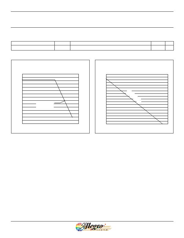
THERMAL CHARACTERISTICS may require derating at maximum conditions, see application information
Characteristic
Symbol
Test Conditions*
Value Units
Package Thermal Resistance
R
窲A
Minimum-K PCB (single-sided with copper limited to solder pads) 177 篊/W
*In still air. Additional thermal information available on Allegro Web site.
20 40 60 80 100 120 140 160 180
8
10
12
14
0
2
4
6
16
18
20
22
24
26
28
30
(R
JA
= 177 篊/W)
Minimum-K PCB
V
CC(min)
V
CC(max)
20 40 60 80 100 120 140 160 180
Temperature (癈)
(
R
J
A
=
1
7
7
?/DIV>
C
/
W
)
M
i
n
i
m
u
m
-
K
P
C
B
0
50
100
150
200
250
300
350
400
450
500
550
600
650
700
750
800
850
900
The following provide additional information about some of the
parameters cited. For additional information, visit the Allegro
Web site at www.allegromicro.com.
Applied Magnetic Field, B
diff
The differential magnetic flux
density, which is calculated as the arithmetic difference of the
flux densities observed by each of the two Hall elements. f
Bdiff
is
the input signal frequency.
Output Off Switchpoint (Operate Point), B
OP
The value of
increasing differential magnetic flux density at which the device
output switches from low to high (A1421) or high to low (A1422
and A1423).
Output On Switchpoint (Release Point), B
RP
The value of
decreasing differential magnetic flux density at which the device
output switches from high to low (A1421) or from low to high
(A1422 and A1423).
Power-On Time, t
PO
The time needed by the device, after
power is applied, to initialize all circuitry necessary for proper
operation.
Settling Time, t
Settling
The time required by the device, after
t
PO
, and after a valid magnetic signal has been applied, to
provide proper output transitions. Settling time is a function of
magnetic offset, offset polarity, signal phase, signal frequency,
and signal amplitude.
Supply Current (on), I
CC(on)
The current draw of the device
with the output transitor is turned on.
Supply Current (off), I
CC(off)
The current draw of the device
with the output transitor is turned off.
Response Time, t
Response
The total time required for generating
zero-crossing output transitions after initialization (the sum of
Power-on Time and Settling Time).
De nitions of Terms
Power Derating Curve
T
J(max)
= 165癈; I
CC
= I
CC(max)
Maximum Power Dissipation
T
J(max)
= 165癈; I
CC
= I
CC(max)
;
V
CC
= V
CC(max)
相关PDF资料 |
PDF描述 |
|---|---|
| A1425LK | IC SENSOR HALL EFFECT AC 4-SIP |
| A1645LK-I2 | IC SENSOR HALL EFFECT AC 4-SIP |
| A3230LUA-T | IC SW HALL EFFECT CHOPPER 3-SIP |
| A3241LUA-T | IC SWITCH HALL EFFECT 3-SIP |
| A3245LLHLT-T | IC SW HALL EFFECT OMNI SOT23W |
相关代理商/技术参数 |
参数描述 |
|---|---|
| A1422LK-T | 功能描述:IC SENSOR HALL EFFECT AC 4-SIP RoHS:是 类别:传感器,转换器 >> 磁性 - 霍尔效应,数字式开关,线性,罗盘 (IC) 系列:- 标准包装:1 系列:- 传感范围:20mT ~ 80mT 类型:旋转 电源电压:4.5 V ~ 5.5 V 电流 - 电源:15mA 电流 - 输出(最大):- 输出类型:数字式,PWM,8.5 位串行 特点:可编程 工作温度:-40°C ~ 150°C 封装/外壳:20-SSOP(0.209",5.30mm 宽) 供应商设备封装:20-SSOP 包装:Digi-Reel® 其它名称:AS5132-HSST-500DKR |
| A1423 | 制造商:ALLEGRO 制造商全称:Allegro MicroSystems 功能描述:High Precision Hall Effect AC-Coupled Differential Sensor with Integrated Filter Capacitor |
| A14233-000 | 制造商:TE Connectivity 功能描述:HT-SCE-1/4-2.0-9-PB-CS7783 - Bulk |
| A1-423-401-01 | 制造商:HECON / DANAHER 功能描述: |
| A1423LK | 制造商:ALLEGRO 制造商全称:Allegro MicroSystems 功能描述:High Accuracy Analog Speed Sensor with Integrated Filter Capacitor |
发布紧急采购,3分钟左右您将得到回复。