- 您现在的位置:买卖IC网 > PDF目录294783 > A1460A-1TQG176C FPGA, 848 CLBS, 6000 GATES, 125 MHz, PQFP176 PDF资料下载
参数资料
| 型号: | A1460A-1TQG176C |
| 元件分类: | FPGA |
| 英文描述: | FPGA, 848 CLBS, 6000 GATES, 125 MHz, PQFP176 |
| 封装: | 1.40 MM HEIGHT, TQFP-176 |
| 文件页数: | 2/68页 |
| 文件大小: | 489K |
| 代理商: | A1460A-1TQG176C |
第1页当前第2页第3页第4页第5页第6页第7页第8页第9页第10页第11页第12页第13页第14页第15页第16页第17页第18页第19页第20页第21页第22页第23页第24页第25页第26页第27页第28页第29页第30页第31页第32页第33页第34页第35页第36页第37页第38页第39页第40页第41页第42页第43页第44页第45页第46页第47页第48页第49页第50页第51页第52页第53页第54页第55页第56页第57页第58页第59页第60页第61页第62页第63页第64页第65页第66页第67页第68页
1-184
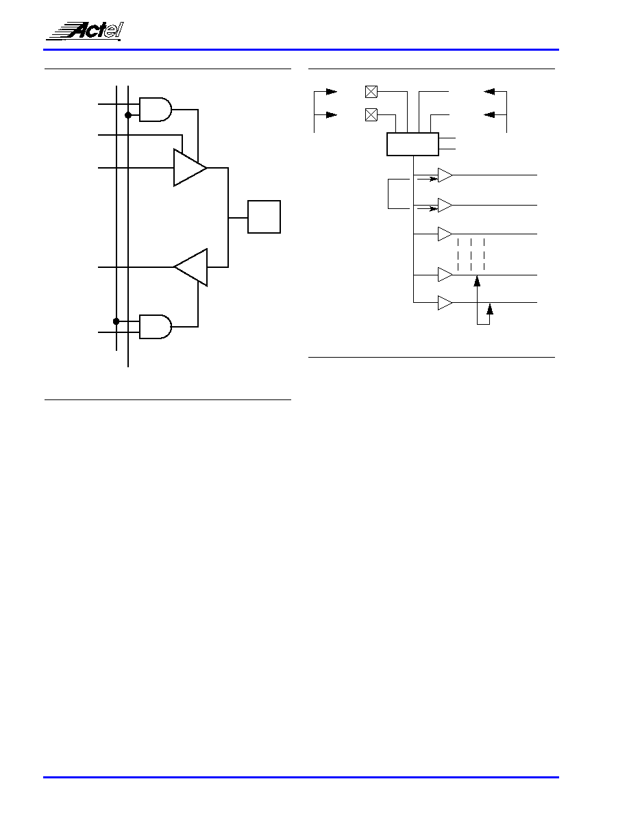
Routed Clocks
The routed clock networks are referred to as CLK0 and CLK1.
Each network is connected to a clock module (CLKMOD)
that selects the source of the clock signal and may be driven
as follows (see Figure 6):
externally from the CLKA pad
externally from the CLKB pad
internally from the CLKINA input
internally from the CLKINB input
The clock modules are located in the top row of I/O modules.
Clock drivers and a dedicated horizontal clock track are
located in each horizontal routing channel. The function of
the clock module is determined by the selection of clock
macros from the macro library. The macro CLKBUF is used to
connect one of the two external clock pins to a clock network,
and the macro CLKINT is used to connect an internally
generated clock signal to a clock network. Since both clock
networks are identical, the user does not care whether CLK0
or CLK1 is being used. Routed clocks can also be used to drive
high fanout nets like resets, output enables, or data enables.
This saves logic modules and results in performance
increases in some cases.
Routing Structure
The ACT 3 architecture uses vertical and horizontal routing
tracks to connect the various logic and I/O modules. These
routing tracks are metal interconnects that may either be of
continuous length or broken into segments. Segments can be
joined together at the ends using antifuses to increase their
lengths up to the full length of the track.
Horizontal Routing
Horizontal channels are located between the rows of modules
and are composed of several routing tracks. The horizontal
routing tracks within the channel are divided into one or
more segments. The minimum horizontal segment length is
the width of a module-pair, and the maximum horizontal
segment length is the full length of the channel. Any segment
that spans more than one-third the row length is considered a
long horizontal segment. A typical channel is shown in
Figure 7. Undedicated horizontal routing tracks are used to
route signal nets. Dedicated routing tracks are used for the
global clock networks and for power and ground tie-off tracks.
Vertical Routing
Other tracks run vertically through the modules. Vertical
tracks are of three types: input, output, and long. Vertical
tracks are also divided into one or more segments. Each
segment in an input track is dedicated to the input of a
particular module. Each segment in an output track is
dedicated to the output of a particular module. Long
segments are uncommitted and can be assigned during
Figure 5 Function Diagram for I/O Pad Driver
PAD
OE
SLEW
DATAOUT
DATAIN
IEN
INEN
OUTEN
Figure 6 Clock Networks
CLKB
CLKA
FROM
PADS
CLOCK
DRIVERS
CLKMOD
CLKINB
CLKINA
S0
S1
INTERNAL
SIGNAL
CLKO(17)
CLKO(16)
CLKO(15)
CLKO(2)
CLKO(1)
CLOCK TRACKS
相关PDF资料 |
PDF描述 |
|---|---|
| A1460A-1TQG176I | FPGA, 848 CLBS, 6000 GATES, PQFP176 |
| A1460A-2PQG160C | FPGA, 848 CLBS, 6000 GATES, 150 MHz, PQFP160 |
| A1460A-2PQG160I | FPGA, 848 CLBS, 6000 GATES, PQFP160 |
| A1460A-2PQG208C | FPGA, 848 CLBS, 6000 GATES, 150 MHz, PQFP208 |
| A1460A-2PQG208I | FPGA, 848 CLBS, 6000 GATES, PQFP208 |
相关代理商/技术参数 |
参数描述 |
|---|---|
| A1460A-1TQG176I | 功能描述:IC FPGA 6K GATES 176-TQFP RoHS:是 类别:集成电路 (IC) >> 嵌入式 - FPGA(现场可编程门阵列) 系列:ACT™ 3 标准包装:1 系列:ProASICPLUS LAB/CLB数:- 逻辑元件/单元数:- RAM 位总计:129024 输入/输出数:248 门数:600000 电源电压:2.3 V ~ 2.7 V 安装类型:表面贴装 工作温度:- 封装/外壳:352-BFCQFP,带拉杆 供应商设备封装:352-CQFP(75x75) |
| A1460A-2PG207C | 制造商:未知厂家 制造商全称:未知厂家 功能描述:Field Programmable Gate Array (FPGA) |
| A1460A-2PQ160C | 制造商:未知厂家 制造商全称:未知厂家 功能描述:Field Programmable Gate Array (FPGA) |
| A1460A-2PQ160I | 制造商:未知厂家 制造商全称:未知厂家 功能描述:Field Programmable Gate Array (FPGA) |
| A1460A-2PQ208C | 制造商: 功能描述: 制造商:undefined 功能描述: |
发布紧急采购,3分钟左右您将得到回复。