- 您现在的位置:买卖IC网 > PDF目录294783 > A1460A-2TQG176C FPGA, 848 CLBS, 6000 GATES, 150 MHz, PQFP176 PDF资料下载
参数资料
| 型号: | A1460A-2TQG176C |
| 元件分类: | FPGA |
| 英文描述: | FPGA, 848 CLBS, 6000 GATES, 150 MHz, PQFP176 |
| 封装: | 1.40 MM HEIGHT, TQFP-176 |
| 文件页数: | 66/68页 |
| 文件大小: | 489K |
| 代理商: | A1460A-2TQG176C |
第1页第2页第3页第4页第5页第6页第7页第8页第9页第10页第11页第12页第13页第14页第15页第16页第17页第18页第19页第20页第21页第22页第23页第24页第25页第26页第27页第28页第29页第30页第31页第32页第33页第34页第35页第36页第37页第38页第39页第40页第41页第42页第43页第44页第45页第46页第47页第48页第49页第50页第51页第52页第53页第54页第55页第56页第57页第58页第59页第60页第61页第62页第63页第64页第65页当前第66页第67页第68页
1-181
Accelerator Series FPGAs – ACT 3 Family
Architecture
This section of the data sheet is meant to familiarize the user
with the architecture of the ACT 3 family of FPGA devices. A
generic description of the family will be presented first,
followed by a detailed description of the logic blocks, the
routing structure, the antifuses, and the special function
circuits. The on-chip circuitry required to program the
devices is not covered.
Topology
The ACT 3 family architecture is composed of six key
elements: Logic modules, I/O modules, I/O Pad Drivers,
Routing Tracks, Clock Networks, and Programming and Test
Circuits. The basic structure is similar for all devices in the
family, differing only in the number of rows, columns, and
I/Os. The array itself consists of alternating rows of modules
and channels. The logic modules and channels are in the
center of the array; the I/O modules are located along the
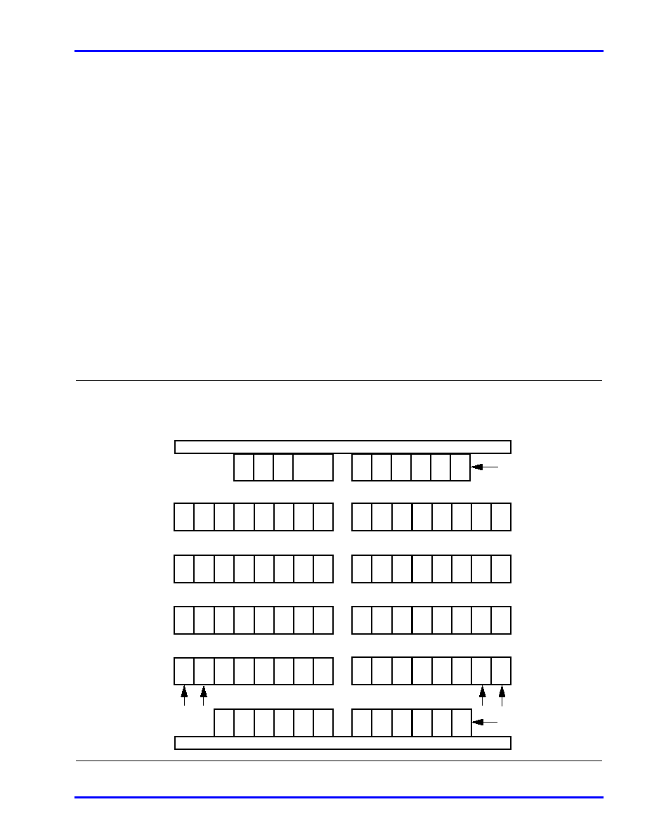
array periphery. A simplified floor plan is depicted in
Logic Modules
ACT 3 logic modules are enhanced versions of the 1200XL
family logic modules. As in the 1200XL family, there are two
types of modules: C-modules and S-modules. The C-module is
functionally equivalent to the 1200XL C-module and
implements high fanin combinatorial macros, such as 5-input
AND, 5-input OR, and so on. It is available for use as the CM8
hard macro. The S-module is designed to implement
high-speed sequential functions within a single module.
S-modules consist of a full C-module driving a flip-flop, which
allows an additional level of logic to be implemented without
additional propagation delay. It is available for use as the
DFM8A/B and DLM8A/B hard macros. C-modules and
S-modules are arranged in pairs called module-pairs.
Module-pairs are arranged in alternating patterns and make
up the bulk of the array. This arrangement allows the
placement software to support two-module macros of four
types (CC, CS, SC, and SS). The C-module implements the
following function:
Y = !S1 * !S0 * D00 + !S1 * S0 * D01 + S1 * !S0 * D10 + S1 * S0
* D11
where: S0 = A0 * B0 and S1 = A1 + B1
Figure 1 Generalized Floor Plan of ACT 3 Device
IO
C
S
C
S
IO
C
S
C
S
IO
C
S
C
S
IO
C
BIO IO
IO
BIN S
C
S
IO
BIN S
C
S
IO
BIN S
C
S
IO
CLKM
IO
BIN S
C
IO
C
S
C
S
C
S
IO
C
An Array with
n rows and m columns
Top I/Os
Bottom I/Os
Left I/Os
Right I/Os
Rows
n+1
n
n–1
2
1
0
Channels
n+1
n
n–1
2
1
0
n+2
0
1
2
3
4
5
c–1
c
c+1
m m+1 m+2 m+3
Columns
相关PDF资料 |
PDF描述 |
|---|---|
| A1460A-2TQG176I | FPGA, 848 CLBS, 6000 GATES, PQFP176 |
| A1460A-3PQG160C | FPGA, 848 CLBS, 6000 GATES, 200 MHz, PQFP160 |
| A1460A-3PQG160I | FPGA, 848 CLBS, 6000 GATES, PQFP160 |
| A1460A-3PQG208C | FPGA, 848 CLBS, 6000 GATES, 200 MHz, PQFP208 |
| A1460A-3TQG176C | FPGA, 848 CLBS, 6000 GATES, 200 MHz, PQFP176 |
相关代理商/技术参数 |
参数描述 |
|---|---|
| A1460A-3PG207C | 制造商:未知厂家 制造商全称:未知厂家 功能描述:Field Programmable Gate Array (FPGA) |
| A1460A-3PQ160C | 制造商:未知厂家 制造商全称:未知厂家 功能描述:Field Programmable Gate Array (FPGA) |
| A1460A-3PQ160I | 制造商:未知厂家 制造商全称:未知厂家 功能描述:Field Programmable Gate Array (FPGA) |
| A1460A-3PQ208C | 制造商:未知厂家 制造商全称:未知厂家 功能描述:Field Programmable Gate Array (FPGA) |
| A1460A-3PQ208I | 制造商:未知厂家 制造商全称:未知厂家 功能描述:Field Programmable Gate Array (FPGA) |
发布紧急采购,3分钟左右您将得到回复。