参数资料
| 型号: | A3P030-2VQG100I |
| 厂商: | Microsemi SoC |
| 文件页数: | 90/220页 |
| 文件大小: | 0K |
| 描述: | IC FPGA 1KB FLASH 30K 100-VQFP |
| 标准包装: | 90 |
| 系列: | ProASIC3 |
| 输入/输出数: | 77 |
| 门数: | 30000 |
| 电源电压: | 1.425 V ~ 1.575 V |
| 安装类型: | 表面贴装 |
| 工作温度: | -40°C ~ 85°C |
| 封装/外壳: | 100-TQFP |
| 供应商设备封装: | 100-VQFP(14x14) |
第1页第2页第3页第4页第5页第6页第7页第8页第9页第10页第11页第12页第13页第14页第15页第16页第17页第18页第19页第20页第21页第22页第23页第24页第25页第26页第27页第28页第29页第30页第31页第32页第33页第34页第35页第36页第37页第38页第39页第40页第41页第42页第43页第44页第45页第46页第47页第48页第49页第50页第51页第52页第53页第54页第55页第56页第57页第58页第59页第60页第61页第62页第63页第64页第65页第66页第67页第68页第69页第70页第71页第72页第73页第74页第75页第76页第77页第78页第79页第80页第81页第82页第83页第84页第85页第86页第87页第88页第89页当前第90页第91页第92页第93页第94页第95页第96页第97页第98页第99页第100页第101页第102页第103页第104页第105页第106页第107页第108页第109页第110页第111页第112页第113页第114页第115页第116页第117页第118页第119页第120页第121页第122页第123页第124页第125页第126页第127页第128页第129页第130页第131页第132页第133页第134页第135页第136页第137页第138页第139页第140页第141页第142页第143页第144页第145页第146页第147页第148页第149页第150页第151页第152页第153页第154页第155页第156页第157页第158页第159页第160页第161页第162页第163页第164页第165页第166页第167页第168页第169页第170页第171页第172页第173页第174页第175页第176页第177页第178页第179页第180页第181页第182页第183页第184页第185页第186页第187页第188页第189页第190页第191页第192页第193页第194页第195页第196页第197页第198页第199页第200页第201页第202页第203页第204页第205页第206页第207页第208页第209页第210页第211页第212页第213页第214页第215页第216页第217页第218页第219页第220页
ProASIC3 DC and Switching Characteristics
2-4
Revision 13
Internal Power-Up Activation Sequence
1. Core
2. Input buffers
Output buffers, after 200 ns delay from input buffer activation
Thermal Characteristics
Introduction
The temperature variable in the Microsemi Designer software refers to the junction temperature, not the
ambient temperature. This is an important distinction because dynamic and static power consumption
cause the chip junction to be higher than the ambient temperature.
EQ 1 can be used to calculate junction temperature.
TJ = Junction Temperature = T + TA
EQ 1
where:
TA = Ambient Temperature
T = Temperature gradient between junction (silicon) and ambient T = ja * P
P = Power dissipation
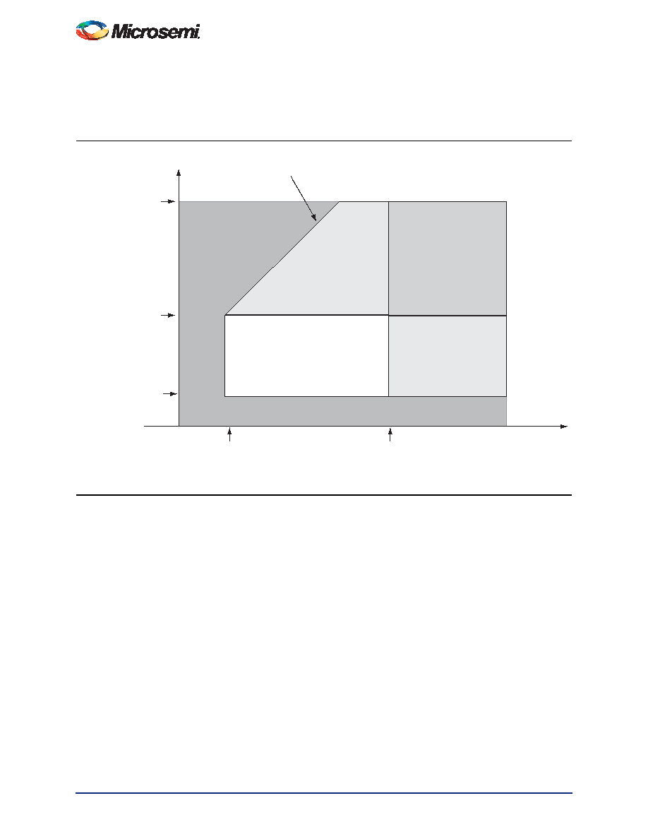
Figure 2-1 I/O State as a Function of VCCI and VCC Voltage Levels
Region 1: I/O buffers are OFF
Region 2: I/O buffers are ON.
I/Os are functional (except differential inputs)
but slower because VCCI / VCC are below
specification. For the same reason, input
buffers do not meet VIH / VIL levels, and
output buffers do not meet VOH / VOL levels.
Min VCCI datasheet specification
voltage at a selected I/O
standard; i.e., 1.425 V or 1.7 V
or 2.3 V or 3.0 V
VCC
VCC = 1.425 V
Region 1: I/O Buffers are OFF
Activation trip point:
Va = 0.85 V ± 0.25 V
Deactivation trip point:
Vd = 0.75 V ± 0.25 V
Activation trip point:
Va = 0.9 V ± 0.3 V
Deactivation trip point:
Vd = 0.8 V ± 0.3 V
VCC = 1.575 V
Region 5: I/O buffers are ON
and power supplies are within
specification.
I/Os meet the entire datasheet
and timer specifications for
speed, VIH / VIL, VOH / VOL,
etc.
Region 4: I/O
buffers are ON.
I/Os are functional
(except differential
but slower because VCCI
is below specification. For the
same reason, input buffers do not
meet VIH / VIL levels, and output
buffers do not meet VOH / VOL levels.
where VT can be from 0.58 V to 0.9 V (typically 0.75 V)
VCCI
Region 3: I/O buffers are ON.
I/Os are functional; I/O DC
specifications are met,
but I/Os are slower because
the VCC is below specification.
VCC = VCCI + VT
相关PDF资料 |
PDF描述 |
|---|---|
| HSC50DREI-S734 | CONN EDGECARD 100POS .100 EYELET |
| ASC40DRTI-S734 | CONN EDGECARD 80POS DIP .100 SLD |
| A3P030-2VQ100I | IC FPGA 1KB FLASH 30K 100-VQFP |
| ASC40DREI-S734 | CONN EDGECARD 80POS .100 EYELET |
| AGL030V5-CSG81I | IC FPGA 1KB FLASH 30K 81-CSP |
相关代理商/技术参数 |
参数描述 |
|---|---|
| A3P030-2VQG144 | 制造商:ACTEL 制造商全称:Actel Corporation 功能描述:ProASIC3 Flash Family FPGAs |
| A3P030-2VQG144ES | 制造商:ACTEL 制造商全称:Actel Corporation 功能描述:ProASIC3 Flash Family FPGAs |
| A3P030-2VQG144I | 制造商:ACTEL 制造商全称:Actel Corporation 功能描述:ProASIC3 Flash Family FPGAs |
| A3P030-2VQG144PP | 制造商:ACTEL 制造商全称:Actel Corporation 功能描述:ProASIC3 Flash Family FPGAs |
| A3P030-DIELOT | 制造商:Microsemi Corporation 功能描述:A3P030-DIELOT - Gel-pak, waffle pack, wafer, diced wafer on film |
发布紧急采购,3分钟左右您将得到回复。