- 您现在的位置:买卖IC网 > PDF目录209983 > A3P030-FVQG100 FPGA, 768 CLBS, 30000 GATES, 350 MHz, PQFP100 PDF资料下载
参数资料
| 型号: | A3P030-FVQG100 |
| 元件分类: | FPGA |
| 英文描述: | FPGA, 768 CLBS, 30000 GATES, 350 MHz, PQFP100 |
| 封装: | 14 X 14 MM, 1 MM HEIGHT, 0.50 MM PITCH, GREEN, VQFP-100 |
| 文件页数: | 2/49页 |
| 文件大小: | 5893K |
| 代理商: | A3P030-FVQG100 |
第1页当前第2页第3页第4页第5页第6页第7页第8页第9页第10页第11页第12页第13页第14页第15页第16页第17页第18页第19页第20页第21页第22页第23页第24页第25页第26页第27页第28页第29页第30页第31页第32页第33页第34页第35页第36页第37页第38页第39页第40页第41页第42页第43页第44页第45页第46页第47页第48页第49页
ProASIC3 DC and Switching Characteristics
v1.3
2 - 83
Clock Conditioning Circuits
CCC Electrical Specifications
Timing Characteristics
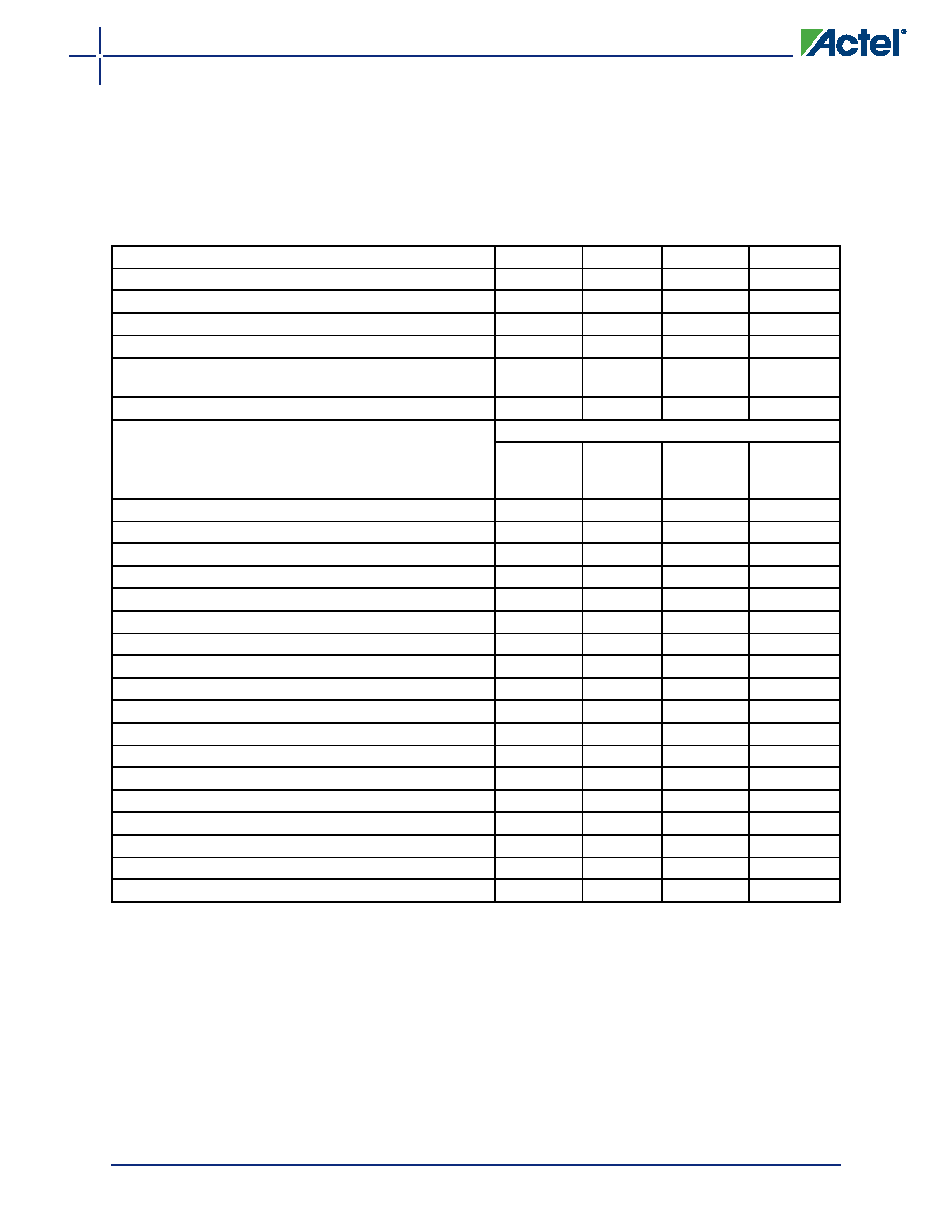
Table 2-106 ProASIC3 CCC/PLL Specification
Parameter
Minimum
Typical
Maximum
Units
Clock Conditioning Circuitry Input Frequency fIN_CCC
1.5
350
MHz
Clock Conditioning Circuitry Output Frequency fOUT_CCC
0.75
350
MHz
Serial Clock (SCLK) for Dynamic PLL1
125
MHz
Delay Increments in Programmable Delay Blocks2, 3
200
ps
Number of Programmable Values in Each Programmable
Delay Block
32
Input Period Jitter
1.5
ns
CCC Output Peak-to-Peak Period Jitter FCCC_OUT
Max Peak-to-Peak Period Jitter
1 Global
Network
Used
3 Global
Networks
Used
0.75 MHz to 24 MHz
0.50%
0.70%
24 MHz to 100 MHz
1.00%
1.20%
100 MHz to 250 MHz
1.75%
2.00%
250 MHz to 350 MHz
2.50%
5.60%
Acquisition Time
(A3P250 and A3P1000 only)
LockControl = 0
300
s
LockControl = 1
300
s
(all other dies)
LockControl = 0
300
s
LockControl = 1
6.0
ms
Tracking Jitter 5
(A3P250 and A3P1000 only)
LockControl = 0
1.6
ns
LockControl = 1
1.6
ns
(all other dies)
LockControl = 0
1.6
ns
LockControl = 1
0.8
ns
Output Duty Cycle
48.5
51.5
%
Delay Range in Block: Programmable Delay 12, 3
0.6
5.56
ns
Delay Range in Block: Programmable Delay 22, 3
0.025
5.56
ns
Delay Range in Block: Fixed Delay2, 3
2.2
ns
Notes:
1. Maximum value obtained for a –2 speed-grade device in worst-case commercial conditions. For specific
junction temperature and voltage supply levels, refer to Table 2-6 on page 2-6 for derating values.
2. This delay is a function of voltage and temperature. See Table 2-6 on page 2-6 for deratings.
3. TJ = 25°C, VCC = 1.5 V
4. The A3P030 device does not contain a PLL.
5. Tracking jitter is defined as the variation in clock edge position of PLL outputs with reference to the PLL
input clock edge. Tracking jitter does not measure the variation in PLL output period, which is covered by
the period jitter parameter.
相关PDF资料 |
PDF描述 |
|---|---|
| A3P125-FFGG144 | FPGA, 3072 CLBS, 125000 GATES, 350 MHz, PBGA144 |
| A3P125-FPQG208 | FPGA, 3072 CLBS, 125000 GATES, 350 MHz, PQFP208 |
| A3P125-FTQG144 | FPGA, 3072 CLBS, 125000 GATES, 350 MHz, PQFP144 |
| A3P125-FVQG100 | FPGA, 3072 CLBS, 125000 GATES, 350 MHz, PQFP100 |
| A42MX36-1BGG304 | FPGA, 2438 CLBS, 36000 GATES, PBGA304 |
相关代理商/技术参数 |
参数描述 |
|---|---|
| A3P030-FVQG144 | 制造商:ACTEL 制造商全称:Actel Corporation 功能描述:ProASIC3 Flash Family FPGAs |
| A3P030-FVQG144ES | 制造商:ACTEL 制造商全称:Actel Corporation 功能描述:ProASIC3 Flash Family FPGAs |
| A3P030-FVQG144I | 制造商:ACTEL 制造商全称:Actel Corporation 功能描述:ProASIC3 Flash Family FPGAs |
| A3P030-FVQG144PP | 制造商:ACTEL 制造商全称:Actel Corporation 功能描述:ProASIC3 Flash Family FPGAs |
| A3P030-PQ144 | 制造商:ACTEL 制造商全称:Actel Corporation 功能描述:ProASIC3 Flash Family FPGAs |
发布紧急采购,3分钟左右您将得到回复。