参数资料
| 型号: | A40MX04-1PLG68 |
| 厂商: | Microsemi SoC |
| 文件页数: | 54/142页 |
| 文件大小: | 0K |
| 描述: | IC FPGA MX SGL CHIP 6K 68-PLCC |
| 标准包装: | 19 |
| 系列: | MX |
| 输入/输出数: | 57 |
| 门数: | 6000 |
| 电源电压: | 3 V ~ 3.6 V,4.75 V ~ 5.25 V |
| 安装类型: | 表面贴装 |
| 工作温度: | 0°C ~ 70°C |
| 封装/外壳: | 68-LCC(J 形引线) |
| 供应商设备封装: | 68-PLCC(24.23x24.23) |
第1页第2页第3页第4页第5页第6页第7页第8页第9页第10页第11页第12页第13页第14页第15页第16页第17页第18页第19页第20页第21页第22页第23页第24页第25页第26页第27页第28页第29页第30页第31页第32页第33页第34页第35页第36页第37页第38页第39页第40页第41页第42页第43页第44页第45页第46页第47页第48页第49页第50页第51页第52页第53页当前第54页第55页第56页第57页第58页第59页第60页第61页第62页第63页第64页第65页第66页第67页第68页第69页第70页第71页第72页第73页第74页第75页第76页第77页第78页第79页第80页第81页第82页第83页第84页第85页第86页第87页第88页第89页第90页第91页第92页第93页第94页第95页第96页第97页第98页第99页第100页第101页第102页第103页第104页第105页第106页第107页第108页第109页第110页第111页第112页第113页第114页第115页第116页第117页第118页第119页第120页第121页第122页第123页第124页第125页第126页第127页第128页第129页第130页第131页第132页第133页第134页第135页第136页第137页第138页第139页第140页第141页第142页
40MX and 42MX FPGA Families
Re vi s i on 11
1 - 15
JTAG Mode Activation
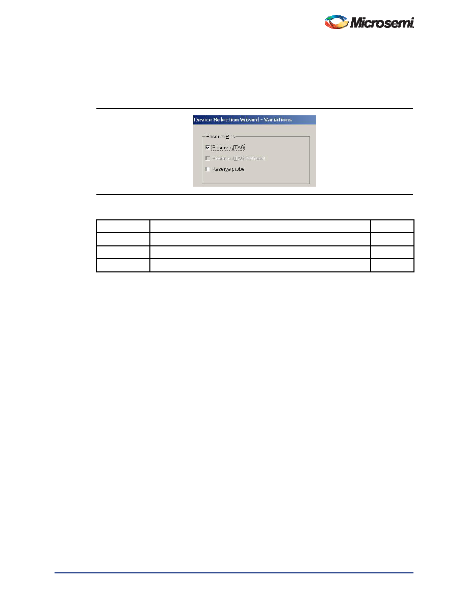
The JTAG test logic circuit is activated in the Designer software by selecting Tools -> Device Selection.
This brings up the Device Selection dialog box as shown in Figure 1-14. The JTAG test logic circuit can
be enabled by clicking the "Reserve JTAG Pins" check box. Table 1-5 explains the pins' behavior in
either mode.
TRST Pin and TAP Controller Reset
An active reset (TRST) pin is not supported; however, MX devices contain power-on circuitry that resets
the boundary scan circuitry upon power-up. Also, the TMS pin is equipped with an internal pull-up
resistor. This allows the TAP controller to remain in or return to the Test-Logic-Reset state when there is
no input or when a logical 1 is on the TMS pin. To reset the controller, TMS must be HIGH for at least five
TCK cycles.
Boundary Scan Description Language (BSDL) File
Conforming to the IEEE Standard 1149.1 requires that the operation of the various JTAG components be
documented. The BSDL file provides the standard format to describe the JTAG components that can be
used by automatic test equipment software. The file includes the instructions that are supported,
instruction bit pattern, and the boundary-scan chain order. For an in-depth discussion on BSDL files,
please refer to Actel BSDL Files Format Description application note.
BSDL files are grouped into two categories - generic and device-specific. The generic files assign all user
I/Os as inouts. Device-specific files assign user I/Os as inputs, outputs or inouts.
Generic files for MX devices are available on the Microsemi SoC Product Group's website:
Figure 1-14 Device Selection Wizard
Table 1-5
Boundary Scan Pin Configuration and Functionality
Reserve JTAG
Checked
Unchecked
TCK
BST input; must be terminated to logical HIGH or LOW to avoid floating
User I/O
TDI, TMS
BST input; may float or be tied to HIGH
User I/O
TDO
BST output; may float or be connected to TDI of another device
User I/O
相关PDF资料 |
PDF描述 |
|---|---|
| A40MX04-1PL68 | IC FPGA MX SGL CHIP 6K 68-PLCC |
| AGLP125V2-CSG281I | IC FPGA IGLOO PLUS 125K 281-CSP |
| AGLP125V2-CS281I | IC FPGA IGLOO PLUS 125K 281-CSP |
| EP4CE15F17I8L | IC CYCLONE IV FPGA 15K 256FBGA |
| EP4CE15F17I7 | IC CYCLONE IV FPGA 15K 256FBGA |
相关代理商/技术参数 |
参数描述 |
|---|---|
| A40MX04-1PLG68I | 功能描述:IC FPGA MX SGL CHIP 6K 68-PLCC RoHS:是 类别:集成电路 (IC) >> 嵌入式 - FPGA(现场可编程门阵列) 系列:MX 标准包装:90 系列:ProASIC3 LAB/CLB数:- 逻辑元件/单元数:- RAM 位总计:36864 输入/输出数:157 门数:250000 电源电压:1.425 V ~ 1.575 V 安装类型:表面贴装 工作温度:-40°C ~ 125°C 封装/外壳:256-LBGA 供应商设备封装:256-FPBGA(17x17) |
| A40MX04-1PLG68M | 制造商:Microsemi Corporation 功能描述:FPGA 6K GATES 547 CELLS 96MHZ/160MHZ 0.45UM 3.3V/5V 68PLCC - Rail/Tube 制造商:Microsemi Corporation 功能描述:IC FPGA MX SGL CHIP 6K 68-PLCC 制造商:Microsemi Corporation 功能描述:IC FPGA 57 I/O 68PLCC |
| A40MX04-1PLG84 | 功能描述:IC FPGA MX SGL CHIP 6K 84-PLCC RoHS:是 类别:集成电路 (IC) >> 嵌入式 - FPGA(现场可编程门阵列) 系列:MX 标准包装:90 系列:ProASIC3 LAB/CLB数:- 逻辑元件/单元数:- RAM 位总计:36864 输入/输出数:157 门数:250000 电源电压:1.425 V ~ 1.575 V 安装类型:表面贴装 工作温度:-40°C ~ 125°C 封装/外壳:256-LBGA 供应商设备封装:256-FPBGA(17x17) |
| A40MX04-1PLG84I | 功能描述:IC FPGA MX SGL CHIP 6K 84-PLCC RoHS:是 类别:集成电路 (IC) >> 嵌入式 - FPGA(现场可编程门阵列) 系列:MX 标准包装:90 系列:ProASIC3 LAB/CLB数:- 逻辑元件/单元数:- RAM 位总计:36864 输入/输出数:157 门数:250000 电源电压:1.425 V ~ 1.575 V 安装类型:表面贴装 工作温度:-40°C ~ 125°C 封装/外壳:256-LBGA 供应商设备封装:256-FPBGA(17x17) |
| A40MX04-1PLG84M | 制造商:Microsemi Corporation 功能描述:FPGA 6K GATES 547 CELLS 96MHZ/160MHZ 0.45UM 3.3V/5V 84PLCC - Rail/Tube 制造商:Microsemi Corporation 功能描述:IC FPGA MX SGL CHIP 6K 84-PLCC 制造商:Microsemi Corporation 功能描述:IC FPGA 69 I/O 84PLCC |
发布紧急采购,3分钟左右您将得到回复。