参数资料
| 型号: | A42MX09-1VQG100I |
| 厂商: | Microsemi SoC |
| 文件页数: | 82/142页 |
| 文件大小: | 0K |
| 描述: | IC FPGA MX SGL CHIP 14K 100VQFP |
| 标准包装: | 90 |
| 系列: | MX |
| 输入/输出数: | 83 |
| 门数: | 14000 |
| 电源电压: | 3 V ~ 3.6 V,4.5 V ~ 5.5 V |
| 安装类型: | 表面贴装 |
| 工作温度: | -40°C ~ 85°C |
| 封装/外壳: | 100-TQFP |
| 供应商设备封装: | 100-VQFP(14x14) |
第1页第2页第3页第4页第5页第6页第7页第8页第9页第10页第11页第12页第13页第14页第15页第16页第17页第18页第19页第20页第21页第22页第23页第24页第25页第26页第27页第28页第29页第30页第31页第32页第33页第34页第35页第36页第37页第38页第39页第40页第41页第42页第43页第44页第45页第46页第47页第48页第49页第50页第51页第52页第53页第54页第55页第56页第57页第58页第59页第60页第61页第62页第63页第64页第65页第66页第67页第68页第69页第70页第71页第72页第73页第74页第75页第76页第77页第78页第79页第80页第81页当前第82页第83页第84页第85页第86页第87页第88页第89页第90页第91页第92页第93页第94页第95页第96页第97页第98页第99页第100页第101页第102页第103页第104页第105页第106页第107页第108页第109页第110页第111页第112页第113页第114页第115页第116页第117页第118页第119页第120页第121页第122页第123页第124页第125页第126页第127页第128页第129页第130页第131页第132页第133页第134页第135页第136页第137页第138页第139页第140页第141页第142页
40MX and 42MX FPGA Families
1- 40
R e v i sio n 1 1
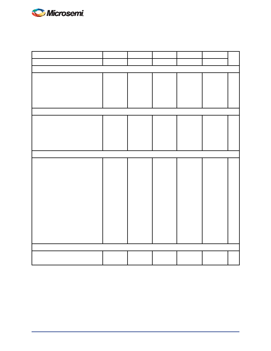
Timing Characteristics
Table 1-28 A40MX02 Timing Characteristics (Nominal 5.0 V Operation)
(Worst-Case Commercial Conditions, VCC = 4.75 V, TJ = 70°C)
–3 Speed
–2 Speed
–1 Speed
Std Speed
–F Speed
Units
Parameter / Description
Min.
Max.
Min.
Max.
Min.
Max.
Min.
Max.
Min.
Max.
Logic Module Propagation Delays
tPD1
Single Module
1.2
1.4
1.6
1.9
2.7
ns
tPD2
Dual-Module Macros
2.7
3.1
3.5
4.1
5.7
ns
tCO
Sequential Clock-to-Q
1.2
1.4
1.6
1.9
2.7
ns
tGO
Latch G-to-Q
1.2
1.4
1.6
1.9
2.7
ns
tRS
Flip-Flop (Latch) Reset-to-Q
1.2
1.4
1.6
1.9
2.7
ns
Logic Module Predicted Routing Delays1
tRD1
FO = 1 Routing Delay
1.3
1.5
1.7
2.0
2.8
ns
tRD2
FO = 2 Routing Delay
1.8
2.1
2.4
2.8
3.9
ns
tRD3
FO = 3 Routing Delay
2.3
2.7
3.0
3.6
5.0
ns
tRD4
FO = 4 Routing Delay
2.9
3.3
3.7
4.4
6.1
ns
tRD8
FO = 8 Routing Delay
4.9
5.7
6.5
7.6
10.6
ns
Logic Module Sequential Timing2
tSUD
Flip-Flop (Latch)
Data Input Set-Up
3.1
3.5
4.0
4.7
6.6
ns
tHD
3
Flip-Flop (Latch)
Data Input Hold
0.0
ns
tSUENA Flip-Flop (Latch)
Enable Set-Up
3.1
3.5
4.0
4.7
6.6
ns
tHENA
Flip-Flop (Latch) Enable Hold
0.0
ns
tWCLKA Flip-Flop (Latch)
Clock Active Pulse Width
3.3
3.8
4.3
5.0
7.0
ns
tWASYN Flip-Flop (Latch)
Asynchronous Pulse Width
3.3
3.8
4.3
5.0
7.0
ns
tA
Flip-Flop Clock Input Period
4.8
5.6
6.3
7.5
10.4
ns
fMAX
Flip-Flop (Latch) Clock
Frequency (FO = 128)
181
168
154
134
80
MHz
Input Module Propagation Delays
tINYH
Pad-to-Y HIGH
0.7
0.8
0.9
1.1
1.5
ns
tINYL
Pad-to-Y LOW
0.6
0.7
0.8
1.0
1.3
ns
Notes:
1. Routing delays are for typical designs across worst-case operating conditions. These parameters should be used for
estimating device performance. Post-route timing analysis or simulation is required to determine actual performance.
2. Set-up times assume fanout of 3. Further testing information can be obtained from the Timer utility.
3. The hold time for the DFME1A macro may be greater than 0 ns. Use the Timer tool from the Designer software to check
the hold time for this macro.
4. Delays based on 35pF loading.
相关PDF资料 |
PDF描述 |
|---|---|
| AMM24DRMD | CONN EDGECARD 48POS .156 WW |
| M1AGL1000V5-FG144 | IC FPGA 1KB FLASH 1M 144-FBGA |
| M1AGL1000V5-FGG144 | IC FPGA 1KB FLASH 1M 144-FBGA |
| AGL1000V5-FG144 | IC FPGA 1KB FLASH 1M 144FBGA |
| EP4CGX30CF23C8N | IC CYCLONE IV GX FPGA 30K 484FBG |
相关代理商/技术参数 |
参数描述 |
|---|---|
| A42MX09-1VQG100M | 制造商:Microsemi Corporation 功能描述:FPGA 14K GATES 336 CELLS 148MHZ/247MHZ 0.45UM 3.3V/5V 100VQF - Trays 制造商:Microsemi Corporation 功能描述:IC FPGA 83 I/O 100VQFP |
| A42MX09-2BG100 | 制造商:未知厂家 制造商全称:未知厂家 功能描述:40MX and 42MX FPGA Families |
| A42MX09-2BG100A | 制造商:未知厂家 制造商全称:未知厂家 功能描述:40MX and 42MX FPGA Families |
| A42MX09-2BG100B | 制造商:未知厂家 制造商全称:未知厂家 功能描述:40MX and 42MX FPGA Families |
| A42MX09-2BG100ES | 制造商:未知厂家 制造商全称:未知厂家 功能描述:40MX and 42MX FPGA Families |
发布紧急采购,3分钟左右您将得到回复。