参数资料
| 型号: | A42MX16-2PL84 |
| 厂商: | Microsemi SoC |
| 文件页数: | 110/142页 |
| 文件大小: | 0K |
| 描述: | IC FPGA MX SGL CHIP 24K 84-PLCC |
| 标准包装: | 16 |
| 系列: | MX |
| 输入/输出数: | 72 |
| 门数: | 24000 |
| 电源电压: | 3 V ~ 3.6 V,4.75 V ~ 5.25 V |
| 安装类型: | 表面贴装 |
| 工作温度: | 0°C ~ 70°C |
| 封装/外壳: | 84-LCC(J 形引线) |
| 供应商设备封装: | 84-PLCC(29.31x29.31) |
第1页第2页第3页第4页第5页第6页第7页第8页第9页第10页第11页第12页第13页第14页第15页第16页第17页第18页第19页第20页第21页第22页第23页第24页第25页第26页第27页第28页第29页第30页第31页第32页第33页第34页第35页第36页第37页第38页第39页第40页第41页第42页第43页第44页第45页第46页第47页第48页第49页第50页第51页第52页第53页第54页第55页第56页第57页第58页第59页第60页第61页第62页第63页第64页第65页第66页第67页第68页第69页第70页第71页第72页第73页第74页第75页第76页第77页第78页第79页第80页第81页第82页第83页第84页第85页第86页第87页第88页第89页第90页第91页第92页第93页第94页第95页第96页第97页第98页第99页第100页第101页第102页第103页第104页第105页第106页第107页第108页第109页当前第110页第111页第112页第113页第114页第115页第116页第117页第118页第119页第120页第121页第122页第123页第124页第125页第126页第127页第128页第129页第130页第131页第132页第133页第134页第135页第136页第137页第138页第139页第140页第141页第142页
40MX and 42MX FPGA Families
Re vi s i on 11
1-3
A42MX24 and A42MX36 devices contain D-modules, which are arranged around the periphery of the
device. D-modules contain wide-decode circuitry, providing a fast, wide-input AND function similar to that
found in CPLD architectures (Figure 1-4). The D-module allows A42MX24 and A42MX36 devices to
perform wide-decode functions at speeds comparable to CPLDs and PALs. The output of the D-module
has a programmable inverter for active HIGH or LOW assertion. The D-module output is hardwired to an
output pin, and can also be fed back into the array to be incorporated into other logic.
Dual-Port SRAM Modules
The A42MX36 device contains dual-port SRAM modules that have been optimized for synchronous or
asynchronous applications. The SRAM modules are arranged in 256-bit blocks that can be configured as
32x8 or 64x4. SRAM modules can be cascaded together to form memory spaces of user-definable width
and depth. A block diagram of the A42MX36 dual-port SRAM block is shown in Figure 1-5.
The A42MX36 SRAM modules are true dual-port structures containing independent read and write ports.
Each SRAM module contains six bits of read and write addressing (RDAD[5:0] and WRAD[5:0],
respectively) for 64x4-bit blocks. When configured in byte mode, the highest order address bits (RDAD5
and WRAD5) are not used. The read and write ports of the SRAM block contain independent clocks
(RCLK and WCLK) with programmable polarities offering active HIGH or LOW implementation. The
SRAM block contains eight data inputs (WD[7:0]), and eight outputs (RD[7:0]), which are connected to
segmented vertical routing tracks.
The A42MX36 dual-port SRAM blocks provide an optimal solution for high-speed buffered applications
requiring FIFO and LIFO queues. The ACTgen Macro Builder within Microsemi's Designer software
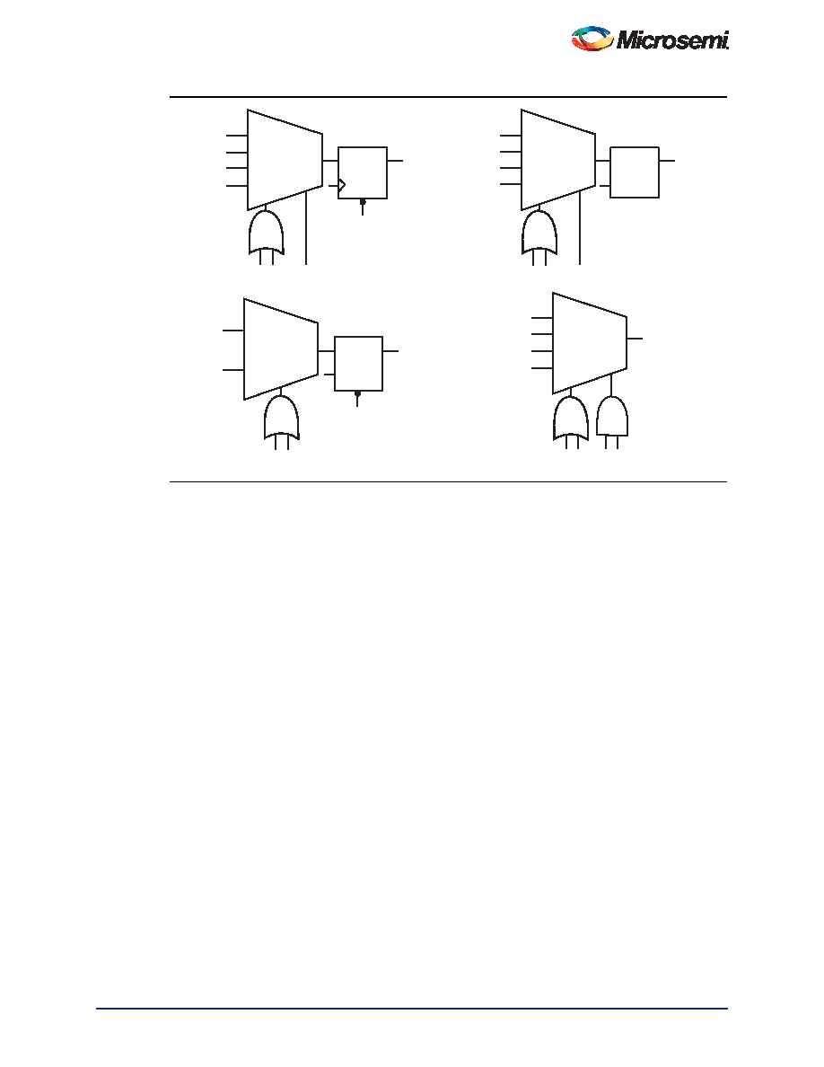
Figure 1-3
42MX S-Module Implementation
CLR
Up to 7-Input Function Plus D-Type Flip-Flop with Clear
Up to 4-Input Function Plus Latch with Clear
D0
D1
S
Y
D
Q
GATE
CLR
OUT
Up to 8-Input Function (Same as C-Module)
D00
D01
D10
D11
S1
S0
Y
OUT
Up to 7-Input Function Plus Latch
D00
D01
D10
D11
S1
S0
Y
OUT
GATE
D
Q
D00
D01
D10
D11
S1
S0
Y
D
Q
OUT
相关PDF资料 |
PDF描述 |
|---|---|
| A42MX16-PQG208A | IC FPGA MX SGL CHIP 24K 208-PQFP |
| 749608-1 | 26 50SR KIT,ST,UK |
| 5745173-4 | CONN BACKSHELL DB25 DIE CAST |
| ABB75DHLR | CONN EDGECARD 150PS .050 DIP SLD |
| RBB105DHAS | CONN EDGE DUAL .050 R/A 210 POS |
相关代理商/技术参数 |
参数描述 |
|---|---|
| A42MX16-2PL84I | 功能描述:IC FPGA MX SGL CHIP 24K 84-PLCC RoHS:否 类别:集成电路 (IC) >> 嵌入式 - FPGA(现场可编程门阵列) 系列:MX 标准包装:40 系列:SX-A LAB/CLB数:6036 逻辑元件/单元数:- RAM 位总计:- 输入/输出数:360 门数:108000 电源电压:2.25 V ~ 5.25 V 安装类型:表面贴装 工作温度:0°C ~ 70°C 封装/外壳:484-BGA 供应商设备封装:484-FPBGA(27X27) |
| A42MX16-2PL84M | 制造商:未知厂家 制造商全称:未知厂家 功能描述:Field Programmable Gate Array (FPGA) |
| A42MX16-2PLG84 | 功能描述:IC FPGA MX SGL CHIP 24K 84-PLCC RoHS:是 类别:集成电路 (IC) >> 嵌入式 - FPGA(现场可编程门阵列) 系列:MX 标准包装:40 系列:SX-A LAB/CLB数:6036 逻辑元件/单元数:- RAM 位总计:- 输入/输出数:360 门数:108000 电源电压:2.25 V ~ 5.25 V 安装类型:表面贴装 工作温度:0°C ~ 70°C 封装/外壳:484-BGA 供应商设备封装:484-FPBGA(27X27) |
| A42MX16-2PLG84I | 功能描述:IC FPGA MX SGL CHIP 24K 84-PLCC RoHS:是 类别:集成电路 (IC) >> 嵌入式 - FPGA(现场可编程门阵列) 系列:MX 标准包装:40 系列:SX-A LAB/CLB数:6036 逻辑元件/单元数:- RAM 位总计:- 输入/输出数:360 门数:108000 电源电压:2.25 V ~ 5.25 V 安装类型:表面贴装 工作温度:0°C ~ 70°C 封装/外壳:484-BGA 供应商设备封装:484-FPBGA(27X27) |
| A42MX16-2PQ100 | 功能描述:IC FPGA MX SGL CHIP 24K 100-PQFP RoHS:否 类别:集成电路 (IC) >> 嵌入式 - FPGA(现场可编程门阵列) 系列:MX 标准包装:40 系列:SX-A LAB/CLB数:6036 逻辑元件/单元数:- RAM 位总计:- 输入/输出数:360 门数:108000 电源电压:2.25 V ~ 5.25 V 安装类型:表面贴装 工作温度:0°C ~ 70°C 封装/外壳:484-BGA 供应商设备封装:484-FPBGA(27X27) |
发布紧急采购,3分钟左右您将得到回复。