参数资料
| 型号: | A42MX16-3PQ160 |
| 厂商: | Microsemi SoC |
| 文件页数: | 112/142页 |
| 文件大小: | 0K |
| 描述: | IC FPGA MX SGL CHIP 24K 160-PQFP |
| 标准包装: | 24 |
| 系列: | MX |
| 输入/输出数: | 125 |
| 门数: | 24000 |
| 电源电压: | 3 V ~ 3.6 V,4.75 V ~ 5.25 V |
| 安装类型: | 表面贴装 |
| 工作温度: | 0°C ~ 70°C |
| 封装/外壳: | 160-BQFP |
| 供应商设备封装: | 160-PQFP(28x28) |
第1页第2页第3页第4页第5页第6页第7页第8页第9页第10页第11页第12页第13页第14页第15页第16页第17页第18页第19页第20页第21页第22页第23页第24页第25页第26页第27页第28页第29页第30页第31页第32页第33页第34页第35页第36页第37页第38页第39页第40页第41页第42页第43页第44页第45页第46页第47页第48页第49页第50页第51页第52页第53页第54页第55页第56页第57页第58页第59页第60页第61页第62页第63页第64页第65页第66页第67页第68页第69页第70页第71页第72页第73页第74页第75页第76页第77页第78页第79页第80页第81页第82页第83页第84页第85页第86页第87页第88页第89页第90页第91页第92页第93页第94页第95页第96页第97页第98页第99页第100页第101页第102页第103页第104页第105页第106页第107页第108页第109页第110页第111页当前第112页第113页第114页第115页第116页第117页第118页第119页第120页第121页第122页第123页第124页第125页第126页第127页第128页第129页第130页第131页第132页第133页第134页第135页第136页第137页第138页第139页第140页第141页第142页
40MX and 42MX FPGA Families
Re vi s i on 11
1 - 67
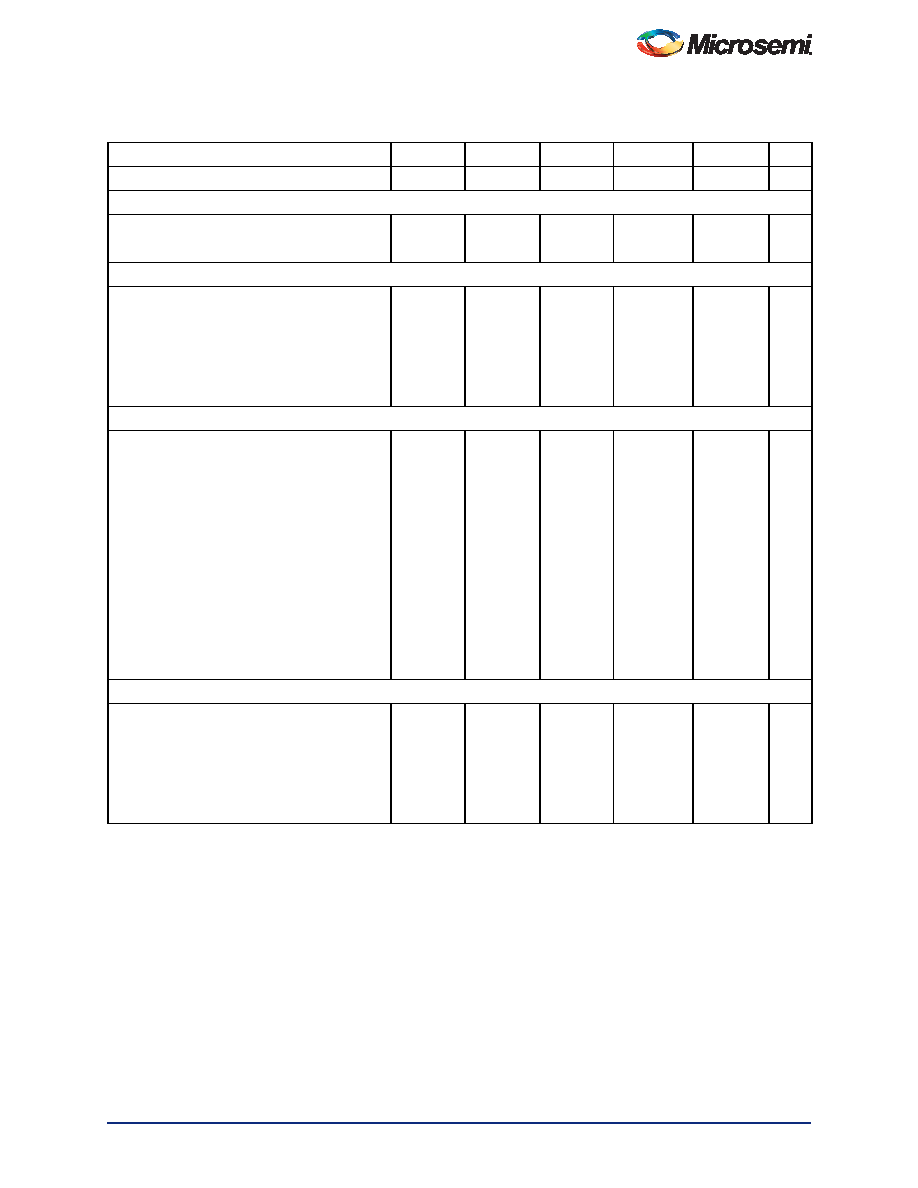
Table 1-36 A42MX24 Timing Characteristics (Nominal 5.0 V Operation)
(Worst-Case Commercial Conditions, VCCA = 4.75 V, TJ = 70°C)
–3 Speed
–2 Speed
–1 Speed
Std Speed
–F Speed
Parameter / Description
Min. Max. Min. Max. Min. Max. Min. Max. Min. Max. Units
Logic Module Combinatorial Functions1
tPD
Internal Array Module Delay
1.2
1.3
1.5
1.8
2.5
ns
tPDD
Internal Decode Module Delay
1.4
1.6
1.8
2.1
3.0
ns
Logic Module Predicted Routing Delays2
tRD1
FO = 1 Routing Delay
0.8
0.9
1.0
1.2
1.7
ns
tRD2
FO = 2 Routing Delay
1.0
1.2
1.3
1.5
2.1
ns
tRD3
FO = 3 Routing Delay
1.3
1.4
1.6
1.9
2.6
ns
tRD4
FO = 4 Routing Delay
1.5
1.7
1.9
2.2
3.1
ns
tRD5
FO = 8 Routing Delay
2.4
2.7
3.0
3.6
5.0
ns
Logic Module Sequential Timing3, 4
tCO
Flip-Flop Clock-to-Output
1.3
1.4
1.6
1.9
2.7
ns
tGO
Latch Gate-to-Output
1.2
1.3
1.5
1.8
2.5
ns
tSUD
Flip-Flop (Latch) Set-Up Time
0.3
0.4
0.5
0.7
ns
tHD
Flip-Flop (Latch) Hold Time
0.0
ns
tRO
Flip-Flop (Latch) Reset-to-Output
1.4
1.6
1.8
2.1
2.9
ns
tSUENA
Flip-Flop (Latch) Enable Set-Up
0.4
0.5
0.6
0.8
ns
tHENA
Flip-Flop (Latch) Enable Hold
0.0
ns
tWCLKA
Flip-Flop (Latch)
Clock Active Pulse Width
3.3
3.7
4.2
4.9
6.9
ns
tWASYN
Flip-Flop (Latch)
Asynchronous Pulse Width
4.4
4.8
5.3
6.5
9.0
ns
Input Module Propagation Delays
tINPY
Input Data Pad-to-Y
1.0
1.1
1.3
1.5
2.1
ns
tINGO
Input Latch Gate-to-Output
1.3
1.4
1.6
1.9
2.6
ns
tINH
Input Latch Hold
0.0
ns
tINSU
Input Latch Set-Up
0.5
0.6
0.7
1.0
ns
tILA
Latch Active Pulse Width
4.7
5.2
5.9
6.9
9.7
ns
Notes:
1. For dual-module macros, use tPD1 + tRD1 + tPDn, tCO + tRD1 + tPDn, or tPD1 + tRD1 + tSUD, whichever is appropriate.
2. Routing delays are for typical designs across worst-case operating conditions. These parameters should be used for
estimating device performance. Post-route timing analysis or simulation is required to determine actual performance.
3. Data applies to macros based on the S-module. Timing parameters for sequential macros constructed from C-modules
can be obtained from the Timer utility.
4. Set-up and hold timing parameters for the Input Buffer Latch are defined with respect to the PAD and the D input.
External setup/hold timing parameters must account for delay from an external PAD signal to the G inputs. Delay from an
external PAD signal to the G input subtracts (adds) to the internal setup (hold) time.
5. Delays based on 35 pF loading.
相关PDF资料 |
PDF描述 |
|---|---|
| HMC49DRTI-S13 | CONN EDGECARD 98POS .100 EXTEND |
| A42MX16-3PQG160 | IC FPGA MX SGL CHIP 24K 160-PQFP |
| A1020B-PQ100I | IC FPGA 2K GATES 100-PQFP IND |
| A1020B-PQG100I | IC FPGA 2K GATES 100-PQFP IND |
| EP20K100EQC240-2X | IC APEX 20KE FPGA 100K 240-PQFP |
相关代理商/技术参数 |
参数描述 |
|---|---|
| A42MX16-3PQ160I | 功能描述:IC FPGA MX SGL CHIP 24K 160-PQFP RoHS:否 类别:集成电路 (IC) >> 嵌入式 - FPGA(现场可编程门阵列) 系列:MX 标准包装:40 系列:SX-A LAB/CLB数:6036 逻辑元件/单元数:- RAM 位总计:- 输入/输出数:360 门数:108000 电源电压:2.25 V ~ 5.25 V 安装类型:表面贴装 工作温度:0°C ~ 70°C 封装/外壳:484-BGA 供应商设备封装:484-FPBGA(27X27) |
| A42MX16-3PQ160M | 制造商:未知厂家 制造商全称:未知厂家 功能描述:Field Programmable Gate Array (FPGA) |
| A42MX16-3PQ208 | 功能描述:IC FPGA MX SGL CHIP 24K 208-PQFP RoHS:否 类别:集成电路 (IC) >> 嵌入式 - FPGA(现场可编程门阵列) 系列:MX 标准包装:40 系列:SX-A LAB/CLB数:6036 逻辑元件/单元数:- RAM 位总计:- 输入/输出数:360 门数:108000 电源电压:2.25 V ~ 5.25 V 安装类型:表面贴装 工作温度:0°C ~ 70°C 封装/外壳:484-BGA 供应商设备封装:484-FPBGA(27X27) |
| A42MX16-3PQ208I | 功能描述:IC FPGA MX SGL CHIP 24K 208-PQFP RoHS:否 类别:集成电路 (IC) >> 嵌入式 - FPGA(现场可编程门阵列) 系列:MX 产品培训模块:Three Reasons to Use FPGA's in Industrial Designs Cyclone IV FPGA Family Overview 特色产品:Cyclone? IV FPGAs 标准包装:60 系列:CYCLONE® IV GX LAB/CLB数:9360 逻辑元件/单元数:149760 RAM 位总计:6635520 输入/输出数:270 门数:- 电源电压:1.16 V ~ 1.24 V 安装类型:表面贴装 工作温度:0°C ~ 85°C 封装/外壳:484-BGA 供应商设备封装:484-FBGA(23x23) |
| A42MX16-3PQ208M | 制造商:未知厂家 制造商全称:未知厂家 功能描述:Field Programmable Gate Array (FPGA) |
发布紧急采购,3分钟左右您将得到回复。