参数资料
| 型号: | A42MX24-1TQG176I |
| 厂商: | Microsemi SoC |
| 文件页数: | 87/142页 |
| 文件大小: | 0K |
| 描述: | IC FPGA MX SGL CHIP 36K 176-TQFP |
| 标准包装: | 40 |
| 系列: | MX |
| 输入/输出数: | 150 |
| 门数: | 36000 |
| 电源电压: | 3 V ~ 3.6 V,4.5 V ~ 5.5 V |
| 安装类型: | 表面贴装 |
| 工作温度: | -40°C ~ 85°C |
| 封装/外壳: | 176-LQFP |
| 供应商设备封装: | 176-TQFP(24x24) |
第1页第2页第3页第4页第5页第6页第7页第8页第9页第10页第11页第12页第13页第14页第15页第16页第17页第18页第19页第20页第21页第22页第23页第24页第25页第26页第27页第28页第29页第30页第31页第32页第33页第34页第35页第36页第37页第38页第39页第40页第41页第42页第43页第44页第45页第46页第47页第48页第49页第50页第51页第52页第53页第54页第55页第56页第57页第58页第59页第60页第61页第62页第63页第64页第65页第66页第67页第68页第69页第70页第71页第72页第73页第74页第75页第76页第77页第78页第79页第80页第81页第82页第83页第84页第85页第86页当前第87页第88页第89页第90页第91页第92页第93页第94页第95页第96页第97页第98页第99页第100页第101页第102页第103页第104页第105页第106页第107页第108页第109页第110页第111页第112页第113页第114页第115页第116页第117页第118页第119页第120页第121页第122页第123页第124页第125页第126页第127页第128页第129页第130页第131页第132页第133页第134页第135页第136页第137页第138页第139页第140页第141页第142页
40MX and 42MX FPGA Families
Re vi s i on 11
1 - 45
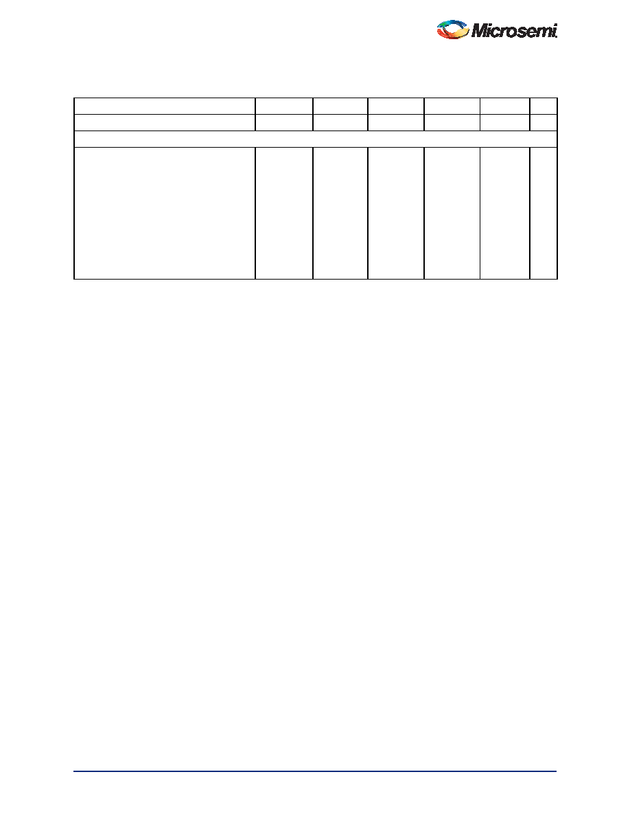
CMOS Output Module Timing4
tDLH
Data-to-Pad HIGH
5.5
6.4
7.2
8.5
11.9
ns
tDHL
Data-to-Pad LOW
4.8
5.5
6.2
7.3
10.2
ns
tENZH
Enable Pad Z to HIGH
4.7
5.5
6.2
7.3
10.2
ns
tENZL
Enable Pad Z to LOW
6.8
7.9
8.9
10.5
14.7
ns
tENHZ
Enable Pad HIGH to Z
11.1
12.8
14.5
17.1
23.9
ns
tENLZ
Enable Pad LOW to Z
8.2
9.5
10.7
12.6
17.7
ns
dTLH
Delta LOW to HIGH
0.05
0.06
0.07
0.10
ns/pF
dTHL
Delta HIGH to LOW
0.03
0.04
0.06
ns/pF
Table 1-29 A40MX02 Timing Characteristics (Nominal 3.3 V Operation) (continued)
(Worst-Case Commercial Conditions, VCC = 3.0 V, TJ = 70°C)
–3 Speed
–2 Speed
–1 Speed
Std Speed
–F Speed
Parameter / Description
Min.
Max.
Min. Max. Min. Max. Min. Max. Min. Max. Units
Notes:
1. Routing delays are for typical designs across worst-case operating conditions. These parameters should be used for
estimating device performance. Post-route timing analysis or simulation is required to determine actual performance.
2. Set-up times assume fanout of 3. Further testing information can be obtained from the Timer utility.
3. The hold time for the DFME1A macro may be greater than 0 ns. Use the Timer tool from the Designer software to check
the hold time for this macro.
4. Delays based on 35 pF loading.
相关PDF资料 |
PDF描述 |
|---|---|
| FMC19DRYI-S13 | CONN EDGECARD 38POS .100 EXTEND |
| A54SX32-TQG144I | IC FPGA SX 48K GATES 144-TQFP |
| A54SX32-1TQG144 | IC FPGA SX 48K GATES 144-TQFP |
| ABM44DRAI | CONN EDGECARD 88POS .156 R/A |
| A54SX32-TQ144I | IC FPGA SX 48K GATES 144-TQFP |
相关代理商/技术参数 |
参数描述 |
|---|---|
| A42MX24-1TQG176M | 制造商:Microsemi Corporation 功能描述:FPGA 42MX Family 36K Gates 912 Cells 0.45um Technology 3.3V/5V 176-Pin TQFP 制造商:Microsemi Corporation 功能描述:FPGA 36K GATES 912 CELLS 0.45UM 3.3V/5V 176TQFP - Trays 制造商:Microsemi Corporation 功能描述:IC FPGA MX SGL CHIP 36K 176-TQFP |
| A42MX24-2PL84 | 功能描述:IC FPGA MX SGL CHIP 36K 84-PLCC RoHS:否 类别:集成电路 (IC) >> 嵌入式 - FPGA(现场可编程门阵列) 系列:MX 产品培训模块:Three Reasons to Use FPGA's in Industrial Designs Cyclone IV FPGA Family Overview 特色产品:Cyclone? IV FPGAs 标准包装:60 系列:CYCLONE® IV GX LAB/CLB数:9360 逻辑元件/单元数:149760 RAM 位总计:6635520 输入/输出数:270 门数:- 电源电压:1.16 V ~ 1.24 V 安装类型:表面贴装 工作温度:0°C ~ 85°C 封装/外壳:484-BGA 供应商设备封装:484-FBGA(23x23) |
| A42MX24-2PL84I | 功能描述:IC FPGA MX SGL CHIP 36K 84-PLCC RoHS:否 类别:集成电路 (IC) >> 嵌入式 - FPGA(现场可编程门阵列) 系列:MX 产品培训模块:Three Reasons to Use FPGA's in Industrial Designs Cyclone IV FPGA Family Overview 特色产品:Cyclone? IV FPGAs 标准包装:60 系列:CYCLONE® IV GX LAB/CLB数:9360 逻辑元件/单元数:149760 RAM 位总计:6635520 输入/输出数:270 门数:- 电源电压:1.16 V ~ 1.24 V 安装类型:表面贴装 工作温度:0°C ~ 85°C 封装/外壳:484-BGA 供应商设备封装:484-FBGA(23x23) |
| A42MX24-2PLG84 | 功能描述:IC FPGA MX SGL CHIP 36K 84-PLCC RoHS:是 类别:集成电路 (IC) >> 嵌入式 - FPGA(现场可编程门阵列) 系列:MX 产品培训模块:Three Reasons to Use FPGA's in Industrial Designs Cyclone IV FPGA Family Overview 特色产品:Cyclone? IV FPGAs 标准包装:60 系列:CYCLONE® IV GX LAB/CLB数:9360 逻辑元件/单元数:149760 RAM 位总计:6635520 输入/输出数:270 门数:- 电源电压:1.16 V ~ 1.24 V 安装类型:表面贴装 工作温度:0°C ~ 85°C 封装/外壳:484-BGA 供应商设备封装:484-FBGA(23x23) |
| A42MX24-2PLG84I | 功能描述:IC FPGA MX SGL CHIP 36K 84-PLCC RoHS:是 类别:集成电路 (IC) >> 嵌入式 - FPGA(现场可编程门阵列) 系列:MX 产品培训模块:Three Reasons to Use FPGA's in Industrial Designs Cyclone IV FPGA Family Overview 特色产品:Cyclone? IV FPGAs 标准包装:60 系列:CYCLONE® IV GX LAB/CLB数:9360 逻辑元件/单元数:149760 RAM 位总计:6635520 输入/输出数:270 门数:- 电源电压:1.16 V ~ 1.24 V 安装类型:表面贴装 工作温度:0°C ~ 85°C 封装/外壳:484-BGA 供应商设备封装:484-FBGA(23x23) |
发布紧急采购,3分钟左右您将得到回复。