参数资料
| 型号: | A54SX08-VQ100I |
| 厂商: | Microsemi SoC |
| 文件页数: | 30/64页 |
| 文件大小: | 0K |
| 描述: | IC FPGA SX 12K GATES 100-VQFP |
| 标准包装: | 90 |
| 系列: | SX |
| LAB/CLB数: | 768 |
| 输入/输出数: | 81 |
| 门数: | 12000 |
| 电源电压: | 3 V ~ 3.6 V,4.75 V ~ 5.25 V |
| 安装类型: | 表面贴装 |
| 工作温度: | -40°C ~ 85°C |
| 封装/外壳: | 100-TQFP |
| 供应商设备封装: | 100-VQFP(14x14) |
第1页第2页第3页第4页第5页第6页第7页第8页第9页第10页第11页第12页第13页第14页第15页第16页第17页第18页第19页第20页第21页第22页第23页第24页第25页第26页第27页第28页第29页当前第30页第31页第32页第33页第34页第35页第36页第37页第38页第39页第40页第41页第42页第43页第44页第45页第46页第47页第48页第49页第50页第51页第52页第53页第54页第55页第56页第57页第58页第59页第60页第61页第62页第63页第64页
SX Family FPGAs
1- 32
v3.2
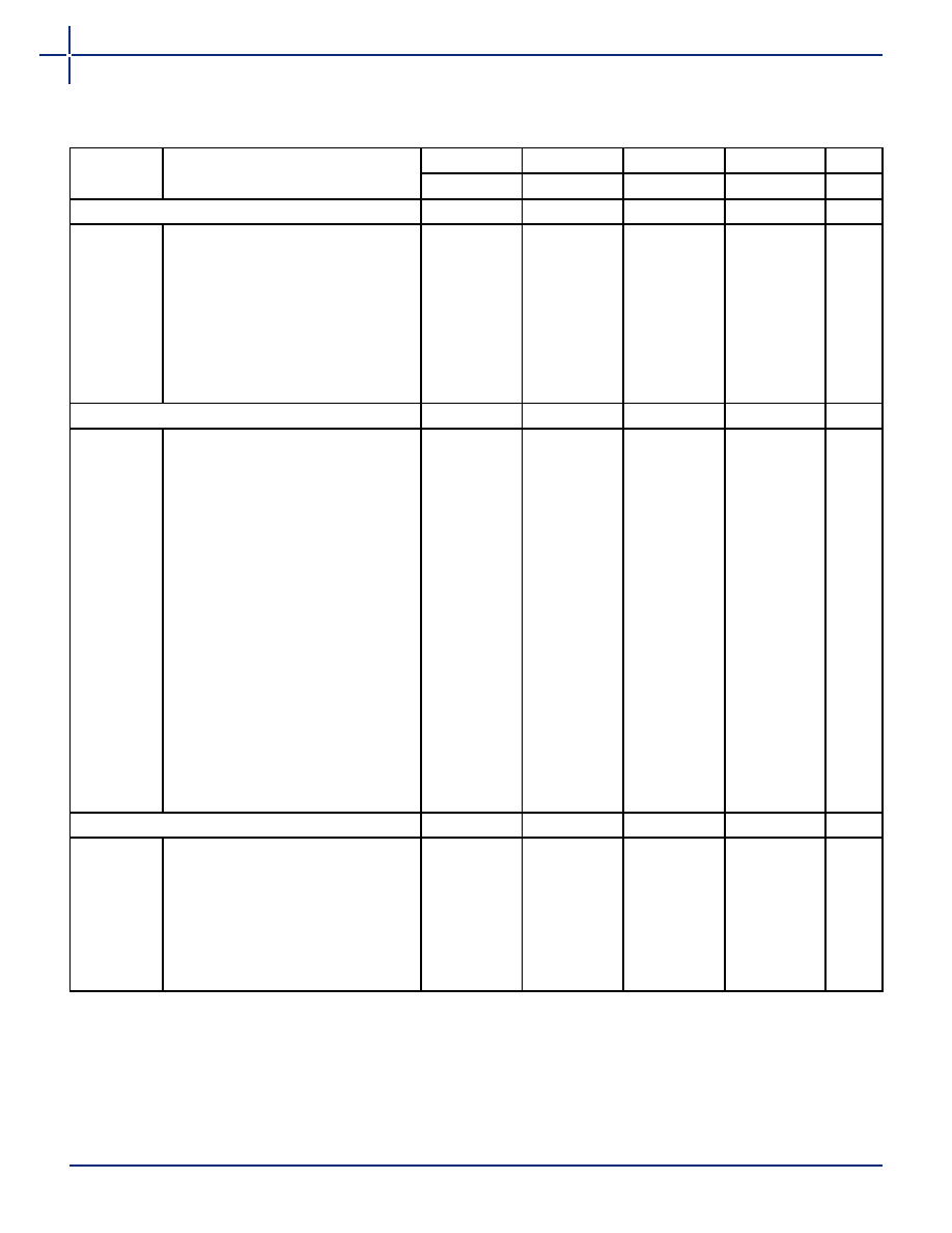
Dedicated (Hardwired) Array Clock Network
tHCKH
Input LOW to HIGH (pad to R-Cell input)
1.9
2.1
2.4
2.8
ns
tHCKL
Input HIGH to LOW (pad to R-Cell input)
1.9
2.1
2.4
2.8
ns
tHPWH
Minimum Pulse Width HIGH
1.4
1.6
1.8
2.1
ns
tHPWL
Minimum Pulse Width LOW
1.4
1.6
1.8
2.1
ns
tHCKSW
Maximum Skew
0.3
0.4
0.5
ns
tHP
Minimum Period
2.7
3.1
3.6
4.2
ns
fHMAX
Maximum Frequency
350
320
280
240
MHz
Routed Array Clock Networks
tRCKH
Input LOW to HIGH (light load)
(pad to R-Cell input)
2.4
2.7
3.0
3.5
ns
tRCKL
Input HIGH to LOW (light load)
(pad to R-Cell input)
2.4
2.7
3.1
3.6
ns
tRCKH
Input LOW to HIGH (50% load)
(pad to R-Cell input)
2.7
3.0
3.5
4.1
ns
tRCKL
Input HIGH to LOW (50% load)
(pad to R-Cell input)
2.7
3.1
3.6
4.2
ns
tRCKH
Input LOW to HIGH (100% load)
(pad to R-Cell input)
2.7
3.1
3.5
4.1
ns
tRCKL
Input HIGH to LOW (100% load)
(pad to R-Cell input)
2.8
3.2
3.6
4.3
ns
tRPWH
Min. Pulse Width HIGH
2.1
2.4
2.7
3.2
ns
tRPWL
Min. Pulse Width LOW
2.1
2.4
2.7
3.2
ns
tRCKSW
Maximum Skew (light load)
0.85
0.98
1.1
1.3
ns
tRCKSW
Maximum Skew (50% load)
1.23
1.4
1.6
1.9
ns
tRCKSW
Maximum Skew (100% load)
1.30
1.5
1.7
2.0
ns
TTL Output Module Timing3
tDLH
Data-to-Pad LOW to HIGH
1.6
1.9
2.1
2.5
ns
tDHL
Data-to-Pad HIGH to LOW
1.6
1.9
2.1
2.5
ns
tENZL
Enable-to-Pad, Z to L
2.1
2.4
2.8
3.2
ns
tENZH
Enable-to-Pad, Z to H
2.3
2.7
3.1
3.6
ns
tENLZ
Enable-to-Pad, L to Z
1.4
1.7
1.9
2.2
ns
tENHZ
Enable-to-Pad, H to Z
1.3
1.5
1.7
2.0
ns
Table 1-20 A54SX32 Timing Characteristics (Continued)
(Worst-Case Commercial Conditions, VCCR= 4.75 V, VCCA,VCCI = 3.0 V, TJ = 70°C)
Parameter
Description
'–3' Speed
'–2' Speed
'–1' Speed
'Std' Speed
Min.
Max.
Min.
Max.
Min.
Max.
Min.
Max.
Units
Note:
1. For dual-module macros, use tPD + tRD1 + tPDn, tRCO + tRD1 + tPDn, or tPD1 + tRD1 + tSUD, whichever is appropriate.
2. Routing delays are for typical designs across worst-case operating conditions. These parameters should be used for estimating
device performance. Post-route timing analysis or simulation is required to determine actual worst-case performance. Post-route
timing is based on actual routing delay measurements performed on the device prior to shipment.
3. Delays based on 35 pF loading, except tENZL and tENZH. For tENZL and tENZH the loading is 5 pF.
相关PDF资料 |
PDF描述 |
|---|---|
| A54SX08-VQG100I | IC FPGA SX 12K GATES 100-VQFP |
| A54SX08-1VQ100 | IC FPGA SX 12K GATES 100-VQFP |
| A54SX08-1VQG100 | IC FPGA SX 12K GATES 100-VQFP |
| A42MX16-PQG208 | IC FPGA MX SGL CHIP 24K 208-PQFP |
| A42MX16-PQ208 | IC FPGA MX SGL CHIP 24K 208-PQFP |
相关代理商/技术参数 |
参数描述 |
|---|---|
| A54SX08-VQ100M | 制造商:未知厂家 制造商全称:未知厂家 功能描述:Field Programmable Gate Array (FPGA) |
| A54SX08-VQ208 | 制造商:未知厂家 制造商全称:未知厂家 功能描述:54SX Family FPGAs |
| A54SX08-VQ208I | 制造商:未知厂家 制造商全称:未知厂家 功能描述:54SX Family FPGAs |
| A54SX08-VQ208M | 制造商:未知厂家 制造商全称:未知厂家 功能描述:54SX Family FPGAs |
| A54SX08-VQ208PP | 制造商:未知厂家 制造商全称:未知厂家 功能描述:54SX Family FPGAs |
发布紧急采购,3分钟左右您将得到回复。