参数资料
| 型号: | A54SX08A-TQG100 |
| 厂商: | Microsemi SoC |
| 文件页数: | 17/108页 |
| 文件大小: | 0K |
| 描述: | IC FPGA 130I/O 100TQFP |
| 标准包装: | 90 |
| 系列: | SX-A |
| LAB/CLB数: | 768 |
| 输入/输出数: | 81 |
| 门数: | 12000 |
| 电源电压: | 2.25 V ~ 5.25 V |
| 安装类型: | 表面贴装 |
| 工作温度: | 0°C ~ 70°C |
| 封装/外壳: | 100-LQFP |
| 供应商设备封装: | 100-TQFP(14x14) |
| 其它名称: | 1100-1064 |
第1页第2页第3页第4页第5页第6页第7页第8页第9页第10页第11页第12页第13页第14页第15页第16页当前第17页第18页第19页第20页第21页第22页第23页第24页第25页第26页第27页第28页第29页第30页第31页第32页第33页第34页第35页第36页第37页第38页第39页第40页第41页第42页第43页第44页第45页第46页第47页第48页第49页第50页第51页第52页第53页第54页第55页第56页第57页第58页第59页第60页第61页第62页第63页第64页第65页第66页第67页第68页第69页第70页第71页第72页第73页第74页第75页第76页第77页第78页第79页第80页第81页第82页第83页第84页第85页第86页第87页第88页第89页第90页第91页第92页第93页第94页第95页第96页第97页第98页第99页第100页第101页第102页第103页第104页第105页第106页第107页第108页
SX-A Family FPGAs
1- 12
v5.3
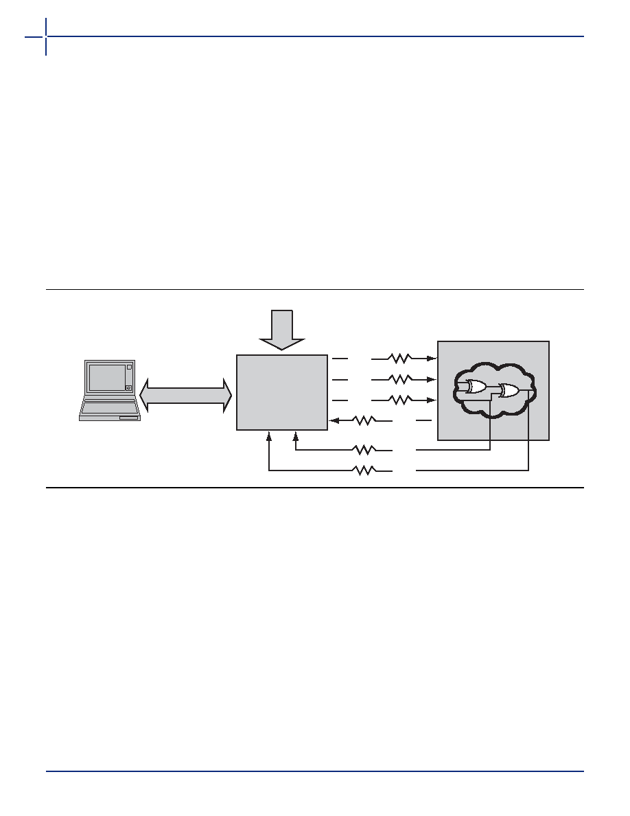
SX-A Probe Circuit Control Pins
SX-A devices contain internal probing circuitry that
provides built-in access to every node in a design,
enabling 100% real-time observation and analysis of a
device's internal logic nodes without design iteration.
The probe circuitry is accessed by Silicon Explorer II, an
easy to use, integrated verification and logic analysis tool
that can sample data at 100 MHz (asynchronous) or
66 MHz (synchronous). Silicon Explorer II attaches to a
PC’s standard COM port, turning the PC into a fully
functional 18-channel logic analyzer. Silicon Explorer II
allows designers to complete the design verification
process at their desks and reduces verification time from
several hours per cycle to a few seconds.
The Silicon Explorer II tool uses the boundary-scan ports
(TDI, TCK, TMS, and TDO) to select the desired nets for
verification. The selected internal nets are assigned to the
PRA/PRB pins for observation. Figure 1-13 illustrates the
interconnection between Silicon Explorer II and the FPGA
to perform in-circuit verification.
Design Considerations
In order to preserve device probing capabilities, users
should avoid using the TDI, TCK, TDO, PRA, and PRB pins
as input or bidirectional ports. Since these pins are active
during probing, critical input signals through these pins
are not available. In addition, the security fuse must not
be programmed to preserve probing capabilities. Actel
recommends that you use a 70
Ω series termination
resistor on every probe connector (TDI, TCK, TMS, TDO,
PRA, PRB). The 70
Ω series termination is used to prevent
data
transmission
corruption
during
probing
and
reading back the checksum.
Figure 1-13 Probe Setup
16
Additional
Channels
SX-A FPGA
70
Ω
70
Ω
70
Ω
70
Ω
70
Ω
70
Ω
TDI
TCK
TMS
TDO
PRA
PRB
Serial Connection
Silicon Explorer II
相关PDF资料 |
PDF描述 |
|---|---|
| M1A3P600L-FG144 | IC FPGA 1KB FLASH 600K 144-FBGA |
| R1EX24128BTAS0A#S0 | IC EEPROM 128K 400KHZ 8TSSOP |
| RMA50DRSD-S288 | CONN EDGECARD 100POS .125 EXTEND |
| HSM36DSAI | CONN EDGECARD 72POS R/A .156 SLD |
| HMM36DSAI | CONN EDGECARD 72POS R/A .156 SLD |
相关代理商/技术参数 |
参数描述 |
|---|---|
| A54SX08A-TQG100A | 功能描述:IC FPGA SX 12K GATES 100-TQFP RoHS:是 类别:集成电路 (IC) >> 嵌入式 - FPGA(现场可编程门阵列) 系列:SX-A 标准包装:90 系列:ProASIC3 LAB/CLB数:- 逻辑元件/单元数:- RAM 位总计:36864 输入/输出数:157 门数:250000 电源电压:1.425 V ~ 1.575 V 安装类型:表面贴装 工作温度:-40°C ~ 125°C 封装/外壳:256-LBGA 供应商设备封装:256-FPBGA(17x17) |
| A54SX08A-TQG100I | 功能描述:IC FPGA SX 12K GATES 100-TQFP RoHS:是 类别:集成电路 (IC) >> 嵌入式 - FPGA(现场可编程门阵列) 系列:SX-A 标准包装:90 系列:ProASIC3 LAB/CLB数:- 逻辑元件/单元数:- RAM 位总计:36864 输入/输出数:157 门数:250000 电源电压:1.425 V ~ 1.575 V 安装类型:表面贴装 工作温度:-40°C ~ 125°C 封装/外壳:256-LBGA 供应商设备封装:256-FPBGA(17x17) |
| A54SX08A-TQG144 | 功能描述:IC FPGA 130I/O 144TQFP RoHS:是 类别:集成电路 (IC) >> 嵌入式 - FPGA(现场可编程门阵列) 系列:SX-A 标准包装:24 系列:ECP2 LAB/CLB数:1500 逻辑元件/单元数:12000 RAM 位总计:226304 输入/输出数:131 门数:- 电源电压:1.14 V ~ 1.26 V 安装类型:表面贴装 工作温度:0°C ~ 85°C 封装/外壳:208-BFQFP 供应商设备封装:208-PQFP(28x28) |
| A54SX08A-TQG144A | 功能描述:IC FPGA SX 12K GATES 144-TQFP RoHS:是 类别:集成电路 (IC) >> 嵌入式 - FPGA(现场可编程门阵列) 系列:SX-A 标准包装:90 系列:ProASIC3 LAB/CLB数:- 逻辑元件/单元数:- RAM 位总计:36864 输入/输出数:157 门数:250000 电源电压:1.425 V ~ 1.575 V 安装类型:表面贴装 工作温度:-40°C ~ 125°C 封装/外壳:256-LBGA 供应商设备封装:256-FPBGA(17x17) |
| A54SX08A-TQG144I | 功能描述:IC FPGA SX 12K GATES 144-TQFP RoHS:是 类别:集成电路 (IC) >> 嵌入式 - FPGA(现场可编程门阵列) 系列:SX-A 标准包装:90 系列:ProASIC3 LAB/CLB数:- 逻辑元件/单元数:- RAM 位总计:36864 输入/输出数:157 门数:250000 电源电压:1.425 V ~ 1.575 V 安装类型:表面贴装 工作温度:-40°C ~ 125°C 封装/外壳:256-LBGA 供应商设备封装:256-FPBGA(17x17) |
发布紧急采购,3分钟左右您将得到回复。